[0014]The transmitting, processing and deriving may be iterated to improve accuracy of relative direction of arrival information derived from the signals at each antenna element after the RFID tag information has been derived. The iterating may include combining the RFID tag information derived from each of a plurality of iterations to form a correlation matrix and applying an algorithm to the correlation matrix to reduce multipath effects in the direction of arrival information for each antenna element. The algorithm may be the MUSIC algorithm.
[0019]A method for deriving information from an RFID tag may include steering first transmitted RFID tag interrogation signals from an array of antenna elements to a first RFID tag, steering second transmitted RFID tag interrogation signals to a second RFID tag, processing signals received by each of the antenna elements from the RFID tag in response to the first and second RFID tag interrogation signals and deriving information from the first and second RFID tag from the processed received signals. The signals received in response to at least one of the transmitted RFID tag interrogation signals may be processed by beamforming to reduce effects of interference in the signals and / or to maximize a ratio of the signals received from the RFID tags compared to interference and noise.
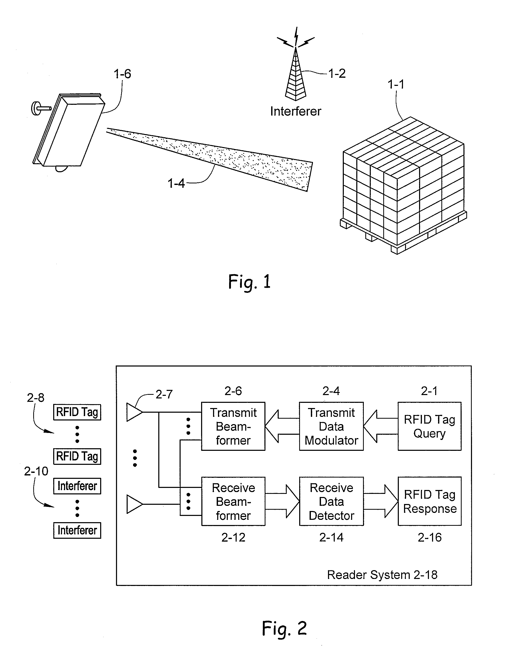
[0024]The digital receive processing block may include a FIR filter providing a first level of FIR filtering for processing the received signals and applying the FIR filter processed signals to the CIC filter wherein the combination of the FIR filter followed by the CIC filter provides a second, higher level of FIR filtering with substantially less complexity than a FIR filter providing the second, higher level of FIR filtering directly. The CIC filter may remove multiple images of a desired received signal portion present in an output of the FIR filter having the first level of FIR filtering. A receive beamformer may be responsive to signals received by each antenna element to combine such received signals to produce and apply a beam steered combined signal to the digital receive processing block to derive RFID tag information from signals received from a first selected direction.
[0026]A dielectric loaded antenna array element may include a dielectric layer, a metallic patch supported on a first side of the dielectric layer, a ground plane layer on an opposite second side of the dielectric layer, antenna feed network connected to antenna terminals and one or more slots in the ground plane layer, coupled to the antenna feed network, for exciting the metallic patch through the dielectric layer, each slot having a narrow central section and an increased area end section at each end of the narrow central section which increases the bandwidth of the antenna element as compared to a constant width slot having the same width as the narrow central section.
[0028]An antenna array element may include an antenna feed network connected to antenna terminals and a square metallic patch driven by the antenna feed network, each side of the patch including a slot having a first end in the center of the edge, a second end towards the center of the patch and an opening in the patch at each second end of each slot to increase the effective electrical length of the antenna array element. The opening at each second end of each slot may be circular or an irregular shape.
[0030]The dielectric may be air. A multilayer printed circuit board may be included having the antenna feed network on a first layer and a ground plane on a second layer, wherein the patch element is supported about the ground plane on the second layer by standoffs so that the space between the ground layer and the patch element serves as the dielectric, and wherein each of the pair of metallic connection elements are bushings having a pin soldered at one end to the antenna feed network, the bushings screwed to the patch element at an other end. Each side of the square metallic patch may have a length and include a slot having a first width, a first end in the center of each such edge, a second end towards the center of the patch and an opening in the patch at each second end of each slot wider than the first width to increase the effective electrical length of the antenna array element beyond the length of the edge.

