Semiconductor package having substrate ID code and its fabricating method

a technology of semiconductor packages and substrates, applied in the direction of manufacturing tools, soldering devices, thermal imaging, etc., can solve the problems of failure tracking and management, and the inability of the id codes of the substrates to provide any information for quality control or failure tracking and management or process improvement of the semiconductor package, so as to increase the complexity of the processing flow

Inactive Publication Date: 2011-02-08
POWERTECH TECHNOLOGY INC
View PDF4 Cites 12 Cited by
  • Summary
  • Abstract
  • Description
  • Claims
  • Application Information

AI Technical Summary

Benefits of technology

[0005]The second purpose of the present invention is to provide a semiconductor package with substrate ID codes and its manufacturing method including a step of flipping the packaged substrate over. Accordingly, the substrate ID code can be formed by laser imprinting at the same time of forming a product code on the encapsulant without adjusting laser beam nor changing laser imprinting machines. The existing laser imprinting machines for semiconductor packaging processes can be implemented without increasing the complexity of the semiconductor packaging processes nor damaging the circuits of the substrates.

Problems solved by technology

Moreover, the substrate cost is increased by putting substrate ID codes on the substrate strip.
However; the ID codes are covered by packaging components such as a chip or an encapsulant during semiconductor packaging processes and can not be recognized by vision inspections.
Therefore, the ID codes of the substrates can not provide any information for quality control or failure tracking and management or process improvement from semiconductor packages.

Method used


Image

  • Semiconductor package having substrate ID code and its fabricating method
  • Semiconductor package having substrate ID code and its fabricating method
  • Semiconductor package having substrate ID code and its fabricating method

Examples


Embodiment Construction

[0015]Please refer to the attached drawings, the present invention will be described by means of embodiments below.

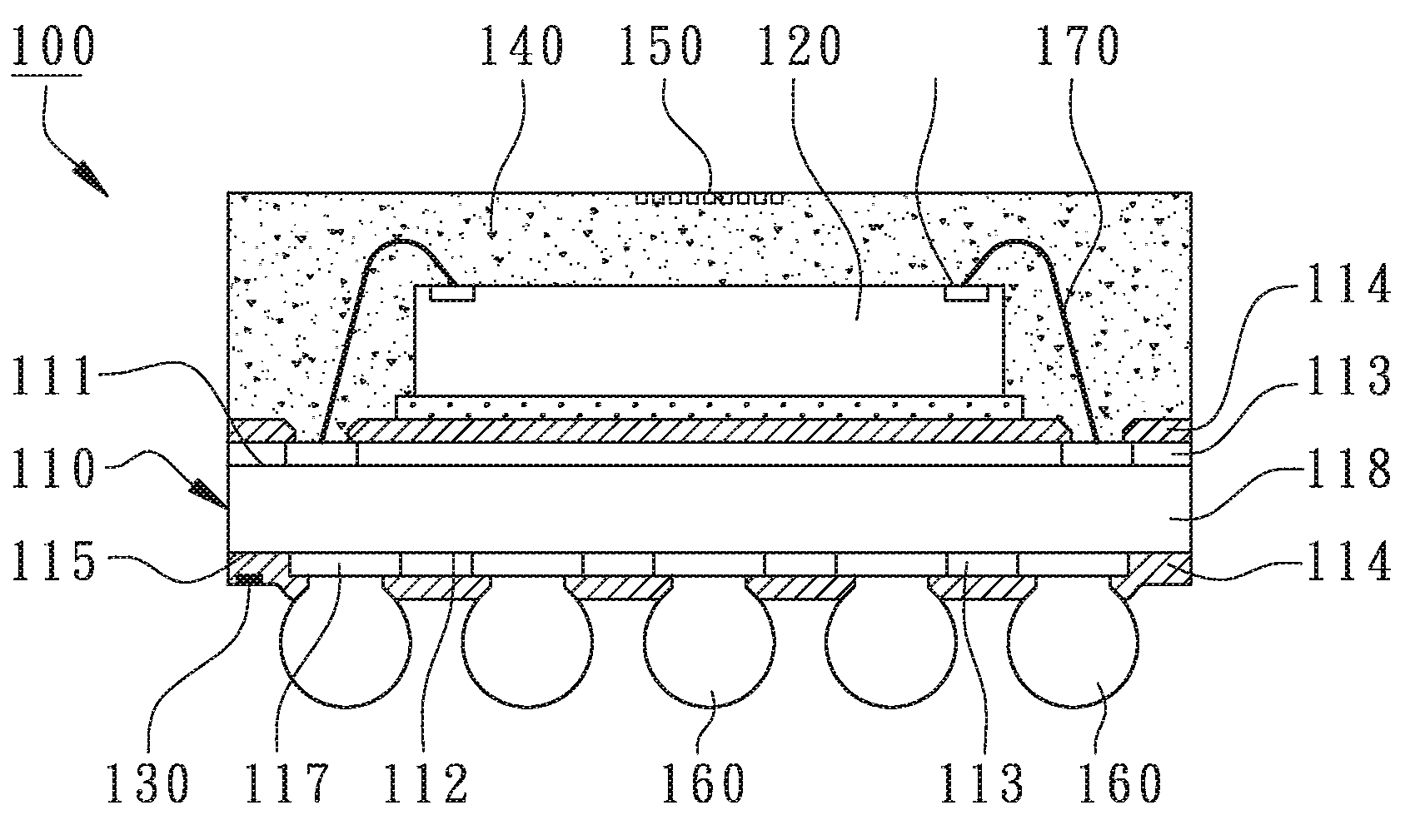
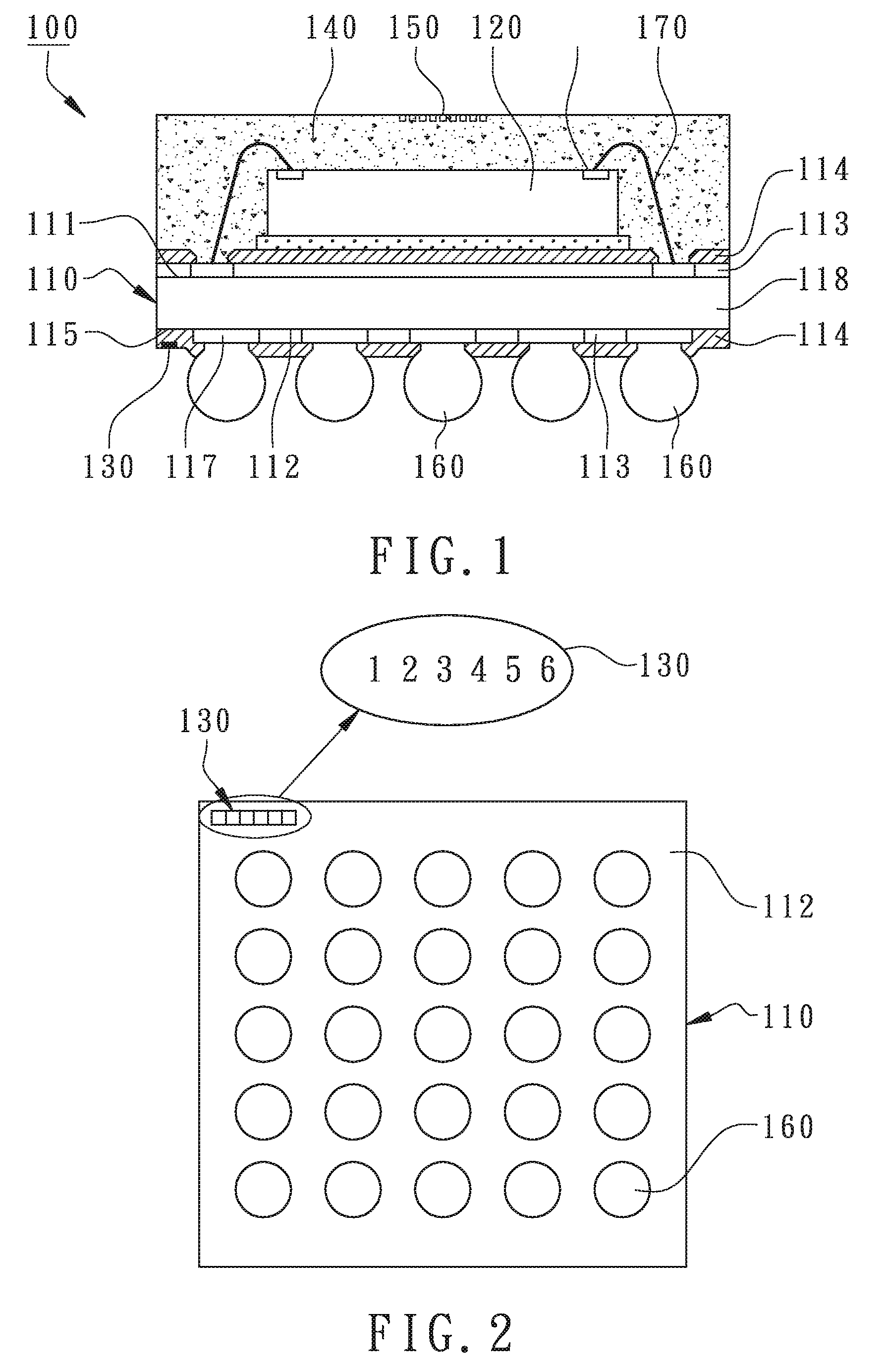
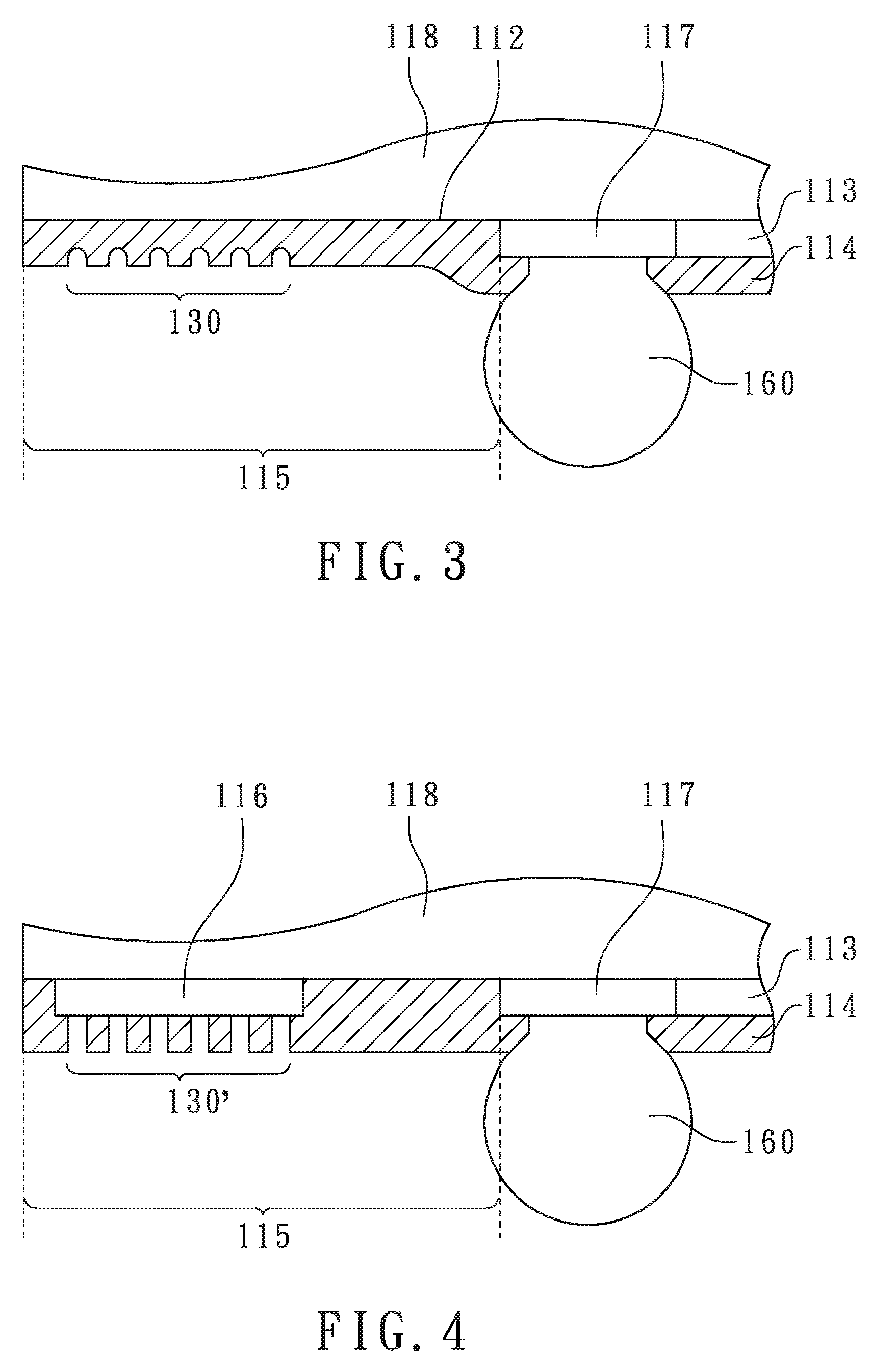
[0016]According to the present invention, a semiconductor package 100 primarily comprises a substrate 110, a chip 120, and a substrate ID code 130 where the substrate 110 has a top surface 111 and a bottom surface 112. The substrate 110 serves as a chip carrier with single-layer or multiple-layer circuits. The substrate 110 includes a circuit 113 and a solder mask 114 formed on the bottom surface 112. In the present embodiment, the substrate 110 is a multiple-layer circuit board further including another circuit 113 and another solder mask 114 formed on the top surface 111. Therein, the circuit 113 on the top surface 111 is electrically connected to the circuit 113 on the bottom surface 112 by a plurality of vias or called PTH's (Plated Through Holes), not shown in figures. The circuit 113 on the top surface 111 includes a plurality of internal pads for electrically con...


PUM

PropertyMeasurementUnit
timeaaaaaaaaaa
areaaaaaaaaaaa
energyaaaaaaaaaa

Abstract

A semiconductor package with a substrate ID code and its manufacturing method are revealed. A circuit and a solder mask are formed on the bottom surface of a substrate where the solder mask covers most of the circuit and a circuit-free zone of the substrate. A chip is disposed on the top surface of the substrate. A substrate ID code consisting of a plurality of laser marks is inscribed in the solder mask or in a portion of an encapsulant on the bottom surface away from the circuit to show the substrate lot number on the bottom surface. Therefore, quality control and failure tracking and management can easily be implemented by tracking the substrate ID code from the semiconductor package without changing the appearance of the semiconductor package. Furthermore, the substrate ID code can be implemented by the existing laser imprinting machines for semiconductor packaging processes and be formed at the same time of formation of a product code. The complexity of the semiconductor packaging processes is not increased and the circuits of the substrates are not easily damaged.

Description

FIELD OF THE INVENTION[0001]The present invention relates to semiconductor devices, especially to a semiconductor package with substrate ID codes and its manufacturing method.BACKGROUND OF THE INVENTION[0002]Substrate strips, or called array packaging substrates and mother substrates, are widely implemented in semiconductor packaging processes as basic packaging components, essentially consisting of a plurality of substrate units from tens to hundreds arranged in multiple arrays. After semiconductor packaging, the arrayed substrates are singulated into individual packages each having one substrate unit. Conventionally, an ID code is disposed on a specific location of the substrate strip outside the substrate units for further production management, quality control, and failure tracking during substrate fabricating processes. However, the ID codes will be removed or covered after the semiconductor packaging processes. Moreover, the substrate cost is increased by putting substrate ID ...

Claims


Application Information

Patent Timeline
Patent Type & Authority Patents(United States)
IPC IPC(8): H01L23/48
CPCB23K1/0016H01L21/67294H01L23/3128H01L23/544H01L24/83B23K35/025B41M5/26H01L23/13H01L23/49816H01L24/85H01L2223/54413H01L2223/54433H01L2223/5448H01L2223/54486H01L2224/16H01L2224/2919H01L2224/48091H01L2224/48228H01L2224/4824H01L2224/73265H01L2224/83101H01L2224/83856H01L2924/15311H01L2924/1815H01L2924/18301H01L2924/00014H01L2924/0665H01L2224/85H01L24/48H01L2224/32225H01L2224/48227H01L2224/73215H01L2924/00012H01L24/73H01L2924/181H01L2224/45099H01L2224/45015H01L2924/207
Inventor CHEN, CHIN-TIHUNG, CHING-WEIYU, BING-SHUNWANG, CHIN-FA
Owner POWERTECH TECHNOLOGY INC
Why Eureka
Try Eureka