Ultrasonic bonding apparatus

a technology of ultrasonic bonding and welding, which is applied in the direction of soldering apparatus, manufacturing tools,auxillary welding devices, etc., can solve the problems of affecting the wiping performance of the tool surface, so as to improve the wiping performance and maintain the tool surface clean. , the effect of improving the wiping performan

Inactive Publication Date: 2011-03-15
FUJITSU LTD
View PDF3 Cites 2 Cited by
  • Summary
  • Abstract
  • Description
  • Claims
  • Application Information

AI Technical Summary

Benefits of technology

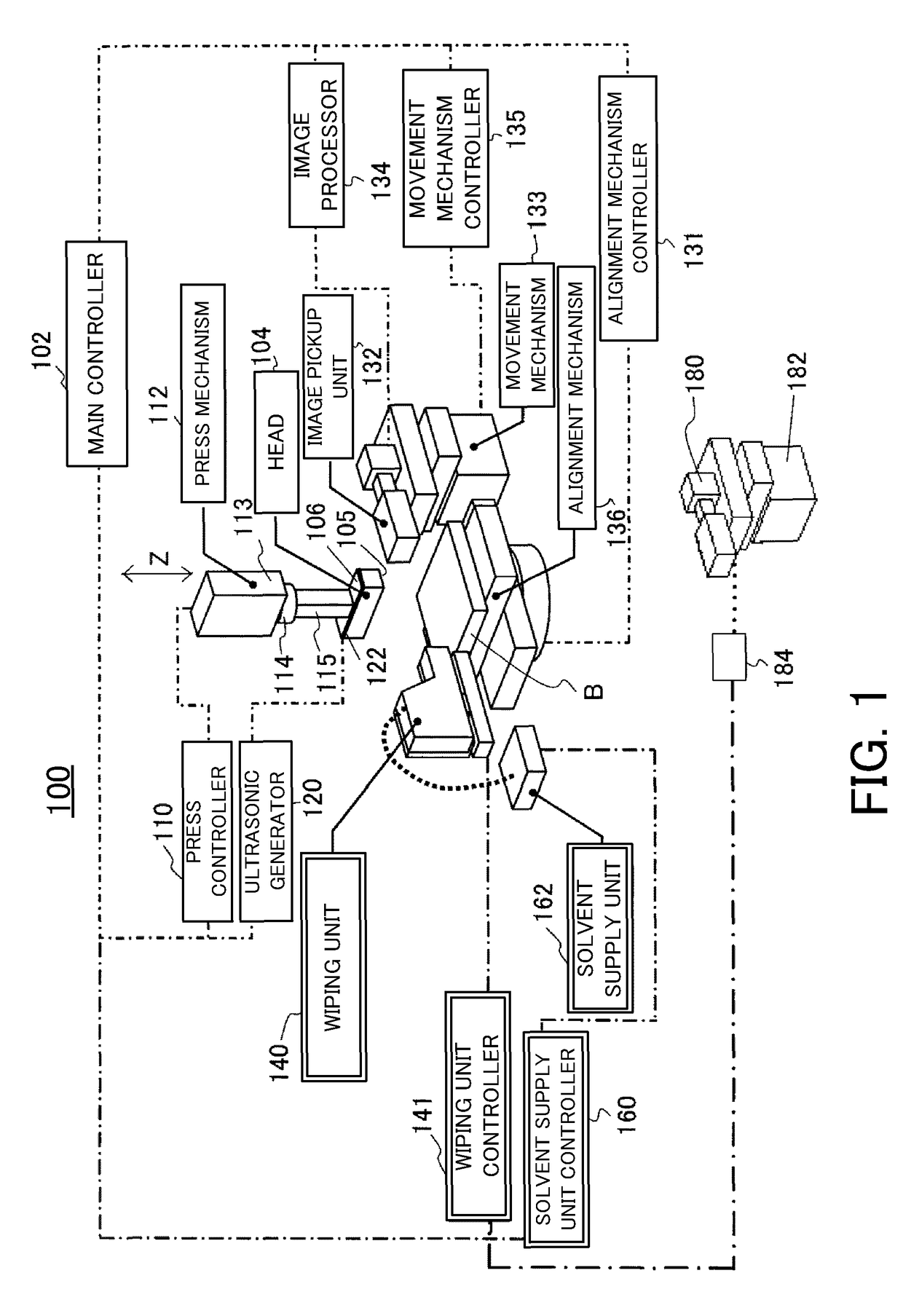
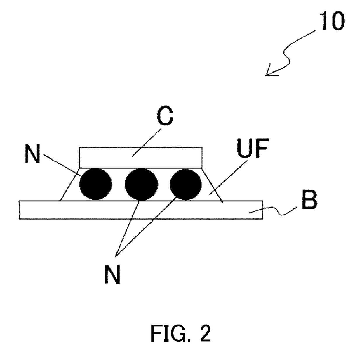
[0011]An ultrasonic bonding apparatus according to one aspect of the present invention used to manufacture an electronic device that includes a substrate, an electronic component, and an underfill that is filled in a space between the electronic component and the substrate includes a head that includes a tool surface configured to mount the electronic component, a wiping unit configured to wipe out pre-cured underfill that has adhered to the tool surface of the head, by using a wiping member on a wiping table, an ultrasonic bonding unit configured to ultrasonically bond the electronic component with the substrate and to press the head against the wiping member on the wiping table, a detector configured to detect a first pressure applied between the wiping member on the wiping table and the tool surface when the wiping unit provides wiping, and a controller configured to control a second pressure applied by the ultrasonic bonding unit, based on a detection result by the detector. This ultrasonic bonding apparatus can maintain the properly set pressure, improve the wiping performance, and maintain the tool surface clean.
[0012]An ultrasonic bonding apparatus according to another aspect of the present invention used to manufacture an electronic device that includes a substrate, an electronic component, and an underfill that is filled in a space between the electronic component and the substrate includes a head that includes a tool surface configured to mount the electronic component, a wiping unit configured to wipe out pre-cured underfill that has adhered to the tool surface of the head, by using a wiping member on a wiping table, the wiping unit including a solvent supply unit configured to supply a solvent configured to powder the underfill, to the wiping member on the wiping table, an ultrasonic bonding unit configured to ultrasonically bond the electronic component with the substrate and to press the head against the wiping member on the wiping table, a detector configured to detect a pressure applied between the wiping member on the wiping table and the tool surface when the wiping unit provides wiping, and controller configured to control a solvent supply amount by the solvent supply unit, based on a detection result by the detector. This ultrasonic bonding apparatus can maintain a solvent supply amount appropriate to the wiping member, improve the wiping performance, and maintain the tool surface clean.
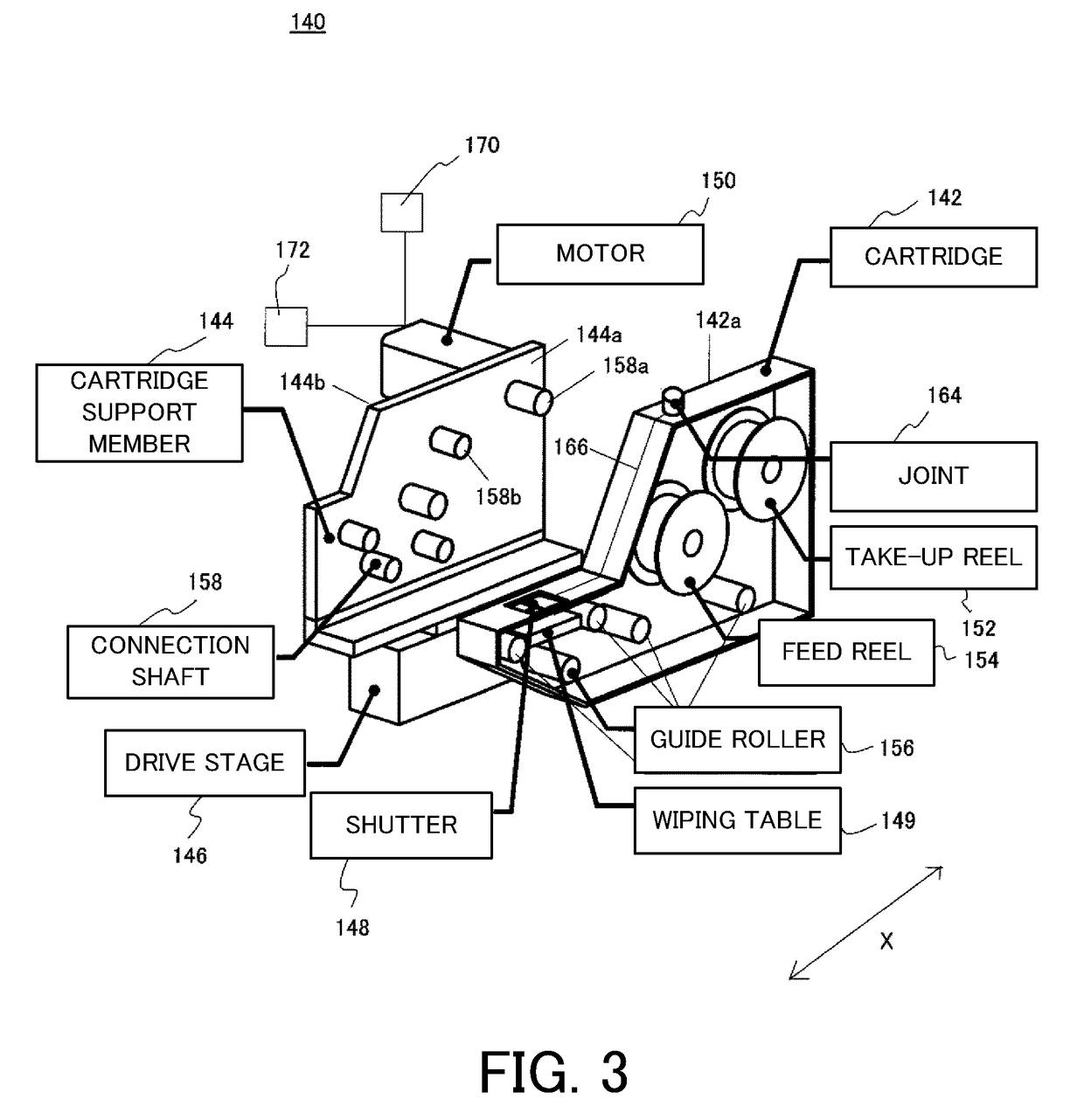
[0013]An ultrasonic bonding apparatus according to still another aspect of the present invention used to manufacture an electronic device that includes a substrate, an electronic component, and an underfill that is filled in a space between the electronic component and the substrate includes a head that includes a tool surface configured to mount the electronic component, a wiping unit configured to wipe out pre-cured underfill that has adhered to the tool surface of the head, by using a wiping member on a wiping table, the wiping unit including a feed mechanism that includes a motor and is configured to supply the wiping member to the wiping table and to roll up the wiping member from the wiping table, an ultrasonic bonding unit configured to ultrasonically bond the electronic component with the substrate, a detector configured to detect a variation of a torque of the motor, and a controller configured to determine whether a residual amount of the wiping member is sufficient, based on a detection result by the detector. This ultrasonic bonding apparatus can recognize a residual amount of the wiping member, avoid wiping when there is no wiping member, and maintains the tool surface clean.
[0014]An ultrasonic bonding apparatus according to another aspect of the present invention used to manufacture an electronic device that includes a substrate, an electronic component, and an underfill that is filled in a space between the electronic component and the substrate includes a head that includes a tool surface configured to mount the electronic component, a wiping unit configured to wipe out pre-cured underfill that has adhered to the tool surface of the head, by using a wiping member on a wiping table, an ultrasonic bonding unit configured to ultrasonically bond the electronic component with the substrate, a detector configured to detect a dirt state on the tool surface by taking an image of a surface of the electronic component that has been bonded with the substrate, and a controller configured to control wiping timing by the wiping unit, based on a detection result by the detector. This ultrasonic bonding apparatus can perform when the tool surface is dirty, and maintain the tool surface clean. When the tool surface is not dirty, the controller can avoid wiping and maintain the throughput of the ultrasonic bonding.

Problems solved by technology

Thus, filling the underfill after mounting (this process will be referred to as “post-filling” of the underfill hereinafter) becomes difficult, and filling the underfill before mounting is necessary (this process will be referred to as “pre-filling” of the underfill hereinafter).
Therefore, the underfill under the chip is forced out in the press time, and adheres to and contaminates the tool surface.
As a result, the parallelism between the chip and the substrate degenerates, and the bonding quality becomes worse.
However, the pre-cured underfill cannot be removed by using the polishing machine because the pre-cured underfill clogs a polishing grindstone.
However, this method can cause a transmission of the ultrasonic vibration to be insufficient, and a slide occurs on both surfaces of the inclusion (film) and the bonding quality becomes unstable.

Method used


Image

  • Ultrasonic bonding apparatus
  • Ultrasonic bonding apparatus
  • Ultrasonic bonding apparatus

Examples


Embodiment Construction

[0042]Referring now to FIGS. 1 and 2, a description will be given of an ultrasonic bonding apparatus 100 according to one aspect of the present invention. FIG. 1 is a block diagram of the ultrasonic bonding apparatus 100. FIG. 2 is a schematic sectional view of the electronic device 10.

[0043]The ultrasonic bonding apparatus 100 is an apparatus used to manufacture the electronic device 10 shown in FIG. 2, and serves to ultrasonically bond a chip (electronic component) C with a substrate B. The electronic device 10 includes a substrate B, a chip C mounted onto or electrically connected to the substrate B via bumps N, and an underfill UF filled in a space between the chip C and the substrate B. More specifically, each bump N is connected to the chip C and the substrate B via a pad (not shown).

[0044]The ultrasonic bonding apparatus 100 includes, as shown in FIG. 1, a main controller 102, a head 104, an ultrasonic bonding unit, an alignment unit, and a wiping unit 140.

[0045]The main cont...


PUM

PropertyMeasurementUnit
pressureaaaaaaaaaa
torqueaaaaaaaaaa
sizeaaaaaaaaaa

Abstract

An ultrasonic bonding apparatus for manufacturing an electronic device that includes a substrate, an electronic component, and an underfill filled between the electronic component and the substrate includes a head that includes a tool surface configured to mount the electronic component, a wiping unit configured to wipe out pre-cured underfill that has adhered to the tool surface of the head, by using a wiping member on a wiping table, an ultrasonic bonding unit configured to ultrasonically bond the electronic component with the substrate and to press the head against the wiping member on the wiping table, a detector configured to detect a first pressure applied between the wiping member on the wiping table and the tool surface when the wiping unit provides wiping, and a controller configured to control a second pressure applied by the ultrasonic bonding unit, based on a detection result by the detector.

Description

[0001]This application is a continuation based on International Application No. PCT / JP2007 / 056562.BACKGROUND OF THE INVENTION[0002]1. Field of the Invention[0003]The present invention relates generally to an ultrasonic bonding (or welding) apparatus, and more particularly to an ultrasonic bonding apparatus configured to fill an underfill in a space between a chip (electronic component) and a substrate, and to bond the chip and the substrate with each other through the underfill. The present invention is suitable, for example, for an ultrasonic bonding apparatus configured to mount a bare chip (flip-chip: FC).[0004]2. Description of the Related Art[0005]Flip-chip mounting is a known technology alternative to wire bonding, which electrically connects a chip to a substrate via an array of bumps. The underfill is filled in a space between the chip and the substrate so as to mitigate an external stress and to improve the reliability of the connection. Recently, as a chip size reduces in ...

Claims


Application Information

Patent Timeline
Patent Type & Authority Patents(United States)
IPC IPC(8): B32B37/00
CPCB23K20/10H01L21/563H01L24/75B23K2201/36H01L2224/16H01L2224/73203H01L2224/75H01L2224/7565H01L2224/757H01L2924/3011H01L2924/3025H01L2924/01005H01L2924/01006H01L2924/01033H01L2924/01074H01L2224/73204H01L2924/00014H01L2924/00011B23K2101/36H01L2224/0401
Inventor MASUDA, YASUYUKIOZAKI, YUKIOMATSUEDA, JUNIKURA, KAZUYUKIKOBAYASHI, TAIZANKASUGA, TOSHINORI
Owner FUJITSU LTD
Why Eureka
Try Eureka