Bias balancing circuit

a bias balancing and circuit technology, applied in the direction of amplifiers, amplifiers with semiconductor devices only, amplifiers, etc., can solve the problems of unsteady voltage sources that easily mislead electronic components into wrong decisions or erroneous judgments, disconnection of electronic devices, and wrong motion of the entire electronic circuit, so as to reduce the number of pins, reduce the cost of ic wafers, and eliminate the influence of offset voltag

Inactive Publication Date: 2011-03-29
AMAZING MICROELECTRONICS
View PDF6 Cites 4 Cited by
  • Summary
  • Abstract
  • Description
  • Claims
  • Application Information

AI Technical Summary

Benefits of technology

[0012]Accordingly, the bias balancing circuit of the invention is to balance the bias while switching input signal sources and eliminate the influence of offset voltage. Thus, the capacitances in the conventional IC wafer for separating the previous and the next bias could be replaced. Moreover, the number of pins could be lessened to decrease the cost of IC wafers considerably.

Problems solved by technology

An unsteady voltage source will easily mislead an electronic component into wrong decision or erroneous judgment in accordance with the logic.
While the input voltage at the gate electrode of n-type MOSFET is unsteady, then n-type MOSFET will easily judge a voltage slightly lower than 3.3 V as a lower level and results in a disconnection of the electronic device and therefore, lead to a wrong motion of the entire electronic circuit.
Additionally, the influence of bias on a digital circuit has an unexpected outcome at the output end caused by the bias.
When the bias is unsteady and the amplifier is not precise enough, the operational amplifier may output irregular waves or cause the distortion of waves.
As for cars, the output voltage of a single battery is 12 V, which is difficult to afford a dual power supply.
Moreover, a dual power supply operational amplifier is more expensive, which means that a single power supply operational amplifier is more suitable for motor sound process wafer 1.
This situation may be caused by the leakage current of the cross-linked capacitance in front of the input buffer inside of the IC wafer, and also weather the circuit layout inside the IC wafer is appropriately operating in coordination or not.
More particularly, because of the mismatch of the circuit layout of internal resistance inside the input buffer of the differential amplifier, the offset voltage is often greater than that of the input buffer of a one-port amplifier.
So, while the bias is affected by the offset voltage to fluctuate, the working region of electronic devices changes with the unsteady bias.
However, in the process of producing IC wafers, the package process occupies a large proportion of cost.

Method used


Image

  • Bias balancing circuit
  • Bias balancing circuit
  • Bias balancing circuit

Examples


Embodiment Construction

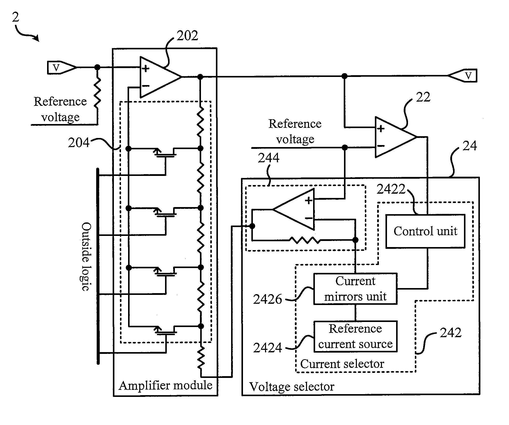
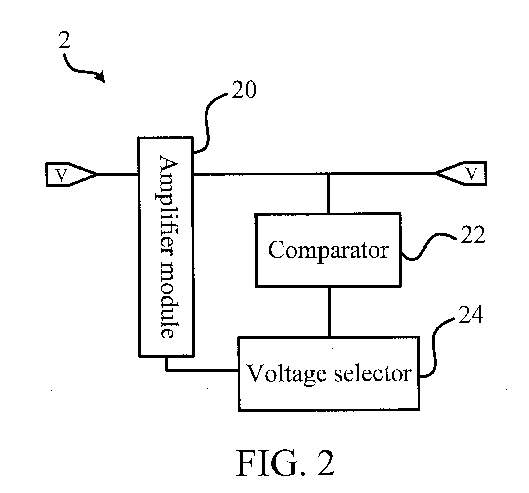
[0020]The present invention provides a bias balancing circuit, and more particularly, the bias balancing circuits of the invention is capable of balancing a bias and eliminates the effect caused by the offset voltage while switching input signal sources. By means of the bias balancing circuit of the present invention, not only the cost of the replaced capacitances could be avoided, but also the number of pins could be lessened to decrease the cost of IC wafer considerably. The objective of the present invention will be illustrated in the following detailed description of the preferred embodiment.

[0021]Please refer to FIG. 2. FIG. 2 is a functional block illustrating a bias balancing circuit 2 according to an embodiment of the invention. As shown in FIG. 2, the main purpose of the bias balancing circuit 2 of the invention is for balancing an output voltage outputted by an amplifier module 20. As everyone knows, the amplifier module 20 changes its variable gain correspondingly while s...


PUM


Abstract

The invention discloses a bias balancing circuit. The bias balancing circuit is used for balancing an output voltage outputted by an amplifier module. The amplifier module has a variable gain. The bias balancing circuit comprises a comparator and a voltage selector. The comparator is used for comparing the output voltage and a reference voltage, to generate a comparison signal. The voltage selector is used for generating a selected voltage according to the comparison signal. When the variable gain is changed to result in an offset from the output voltage to the reference voltage, the bias balancing circuit is capable of balancing the output voltage toward the reference voltage by the selected voltage.

Description

BACKGROUND OF THE INVENTION[0001]1. Field of the Invention[0002]The present invention relates generally to a bias balancing circuit, and more particularly, the bias balancing circuit of the invention is capable of balancing a bias and eliminating the effect caused by the offset voltage while switching input signal sources.[0003]2. Description of the Prior Art[0004]In electronic circuit applications, a steady voltage source and current source often play very important roles. An unsteady voltage source will easily mislead an electronic component into wrong decision or erroneous judgment in accordance with the logic. For example, according to the regulations of a digital circuit, an n-type metal-oxide-semiconductor field-effect transistor (MOSFET) is conducted if the input voltage at the gate electrode of n-type MOSFET is 3.3 V (namely, high level); n-type MOSFET is not conducted if the input voltage is 0 V (namely, low level). While the input voltage at the gate electrode of n-type MO...

Claims


Application Information

Patent Timeline
Patent Type & Authority Patents(United States)
IPC IPC(8): H03G3/12
CPCH03F3/187H03F3/45475H03F3/45991H03F2200/03H03F2200/375H03F2200/78H03F2203/45138H03F2203/45528H03F2203/45534H03F2203/45624
Inventor LIN, WEI-CHENG
Owner AMAZING MICROELECTRONICS
Why Eureka
Try Eureka