Pulse output circuit, shift register, and display device

a shift register and output circuit technology, applied in pulse techniques, generating/distributing signals, instruments, etc., can solve problems such as malfunction, tft b>1020/b> may be turned, and circuit malfunctions, etc., to achieve high frequency, suppress the effect of malfunction of pulse output circuits, and withstand large loads

Active Publication Date: 2011-04-26
SEMICON ENERGY LAB CO LTD
View PDF45 Cites 65 Cited by
  • Summary
  • Abstract
  • Description
  • Claims
  • Application Information

AI Technical Summary

Benefits of technology

[0015]An object of the present invention disclosed in this specification is to provide a pulse output circuit, a shift register, and a display device each of which reduces malfunction in a circuit and assures further reliable operation by solving one or a plurality of such problems.
[0021]In accordance with the present invention, by regularly supplying a potential to a gate electrode of a transistor which is in a floating state during a non-selection period when an input and output of a pulse is not performed, malfunction of a pulse output circuit can be suppressed.
[0022]In addition, by using a driving method in which a pulse outputted from the m-th pulse output circuit overlaps half (½ period) of a pulse outputted from the (m+1)th pulse output circuit, the present invention can provide a pulse output circuit which can withstand large load and operate at high frequency.

Problems solved by technology

As a result, a circuit has a possibility of malfunction due to capacitive coupling with a clock signal.
As a result of this, there is a possibility that the TFT 1020 may be turned on and malfunction may occur.
However, when the potential change is larger than the threshold value of the TFT 1020, malfunction may occur because the potential of the node a decreases.
As a result of this, there is a high possibility that a pulse output circuit may malfunction.
When amorphous silicon is used for a TFT, compared with a TFT using polysilicon, sufficient drive capability is difficult to be obtained because of inferior electric characteristics and a threshold value shifts due to a voltage condition.
Accordingly, a problem is a circuit technique to form a driver circuit which drives a pixel by using a TFT which uses amorphous silicon.

Method used


Image

  • Pulse output circuit, shift register, and display device
  • Pulse output circuit, shift register, and display device
  • Pulse output circuit, shift register, and display device

Examples


embodiment mode 1

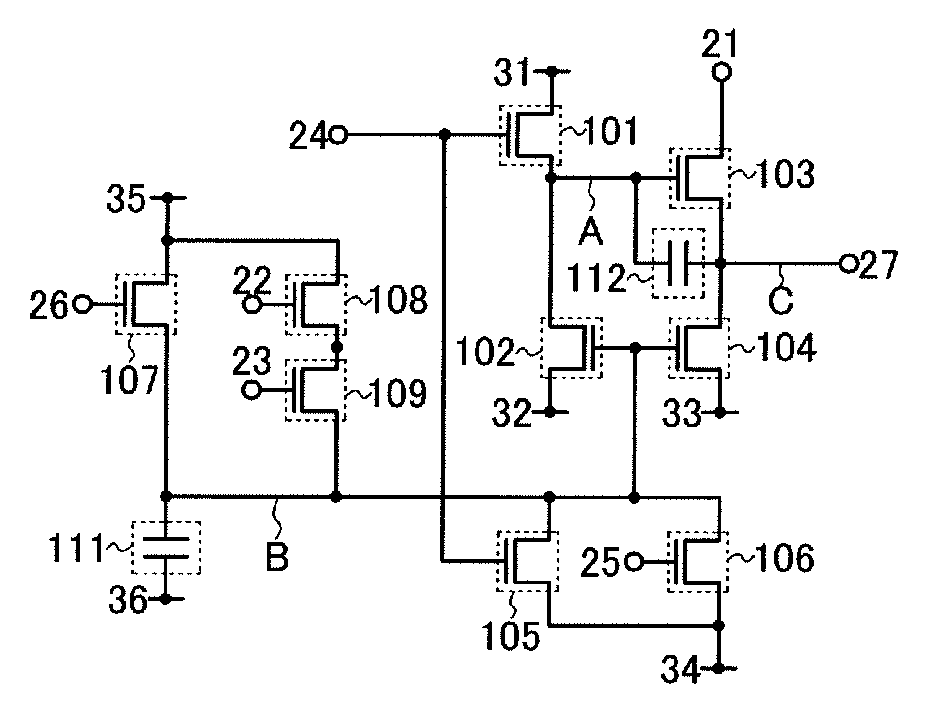
[0039]In this embodiment mode, an example of a pulse output circuit of the present invention and a shift register including the pulse output circuit will be described with reference to drawings.

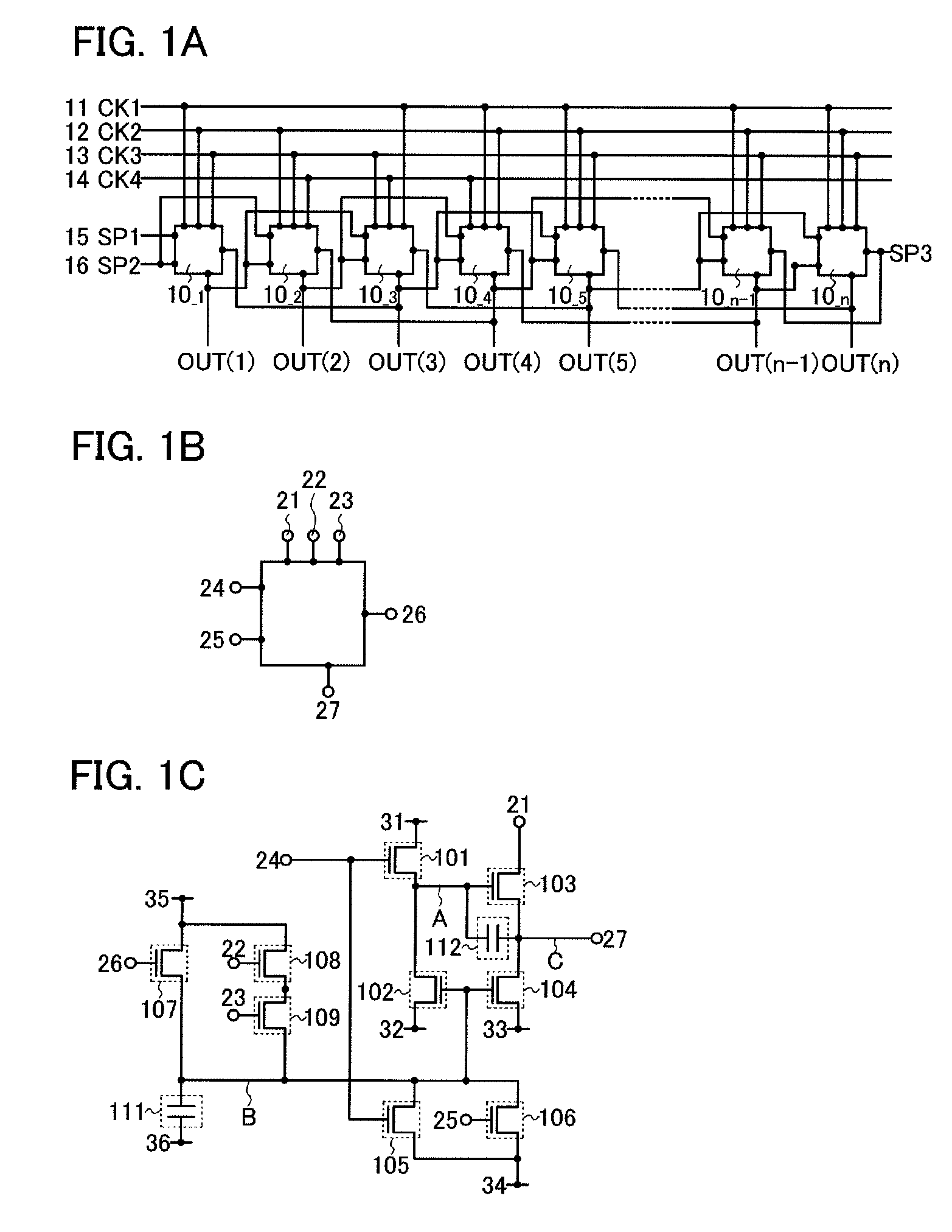
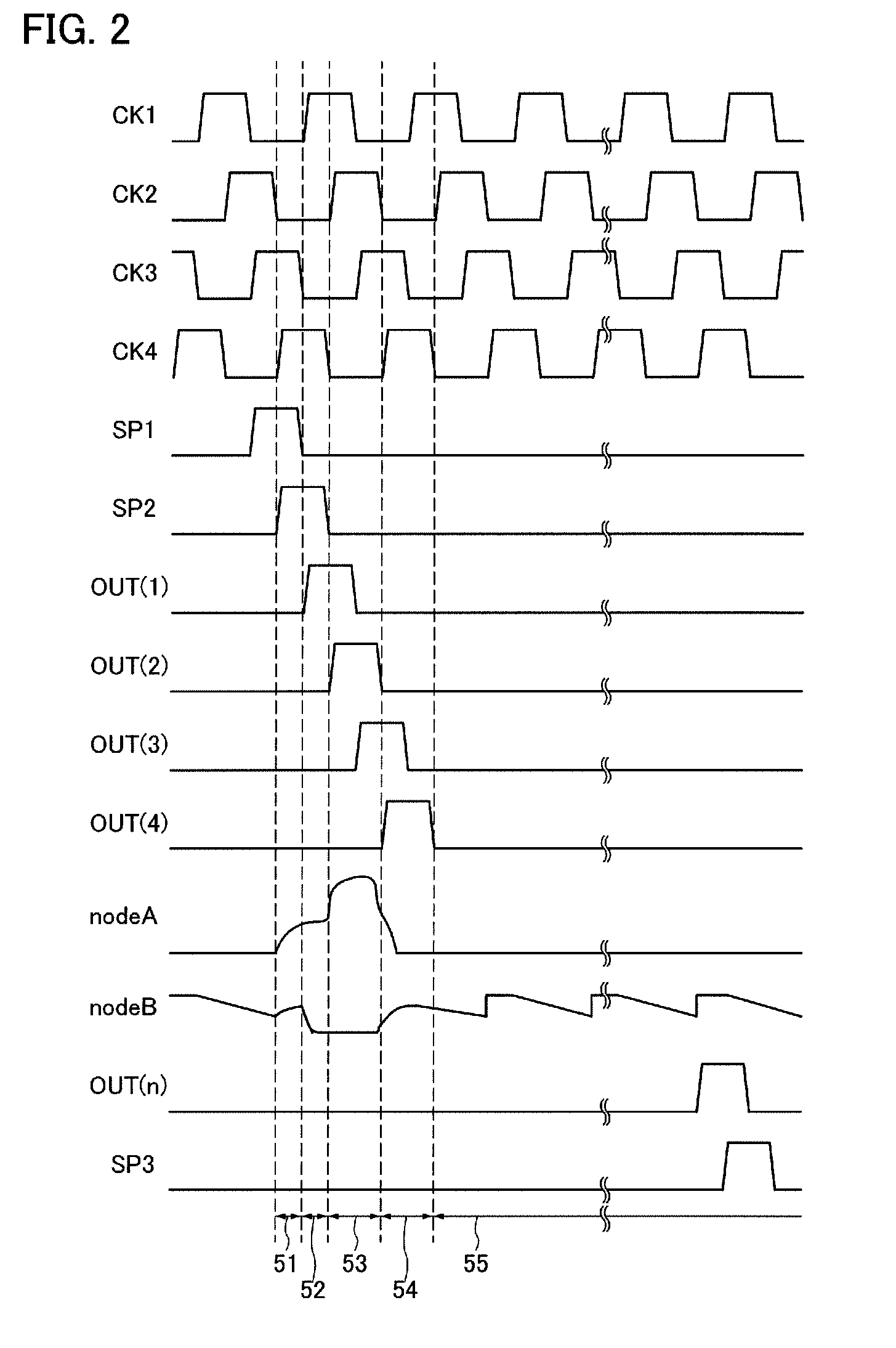
[0040]A shift register shown in this embodiment mode includes first to n-th pulse output circuits 10—1 to 10—n (n≧3) and first to fourth signal lines 11 to 14 each of which outputs a clock signal (see FIG. 1A). The first signal line 11 outputs a first clock signal (CK1), the second signal line 12 outputs a second clock signal (CK2), the third signal line 13 outputs a third clock signal (CK3), and the fourth signal line 14 outputs a fourth clock signal (CK4).

[0041]The clock signals (CK) are signals which alternate between an H (High) signal and an L (Low) signal at a regular interval, and here, the first to fourth clock signals (CK1) to (CK4) are delayed for ½ period sequentially. In this embodiment mode, by using the first to fourth clock signals (CK1) to (CK4), control or the like of driving...

embodiment mode 2

[0073]In this embodiment mode, structures of a shift register and a pulse output circuit which are different from those in the above embodiment mode will be described with reference to drawings.

[0074]A shift register shown in this embodiment mode includes the first to n-th pulse output circuits 10—1 to 10—n (n≧3) and the first to fourth signal lines 11 to 14 each of which outputs a clock signal (see FIG. 6A). In addition, each of the first to n-th pulse output circuits 10—1 to 10—n includes the first input terminal 21, the second input terminal 22, the third input terminal 23, the fourth input terminal 24, the fifth input terminal 25, the sixth input terminal 26, the first output terminal 27, and a second output terminal 28 (see FIG. 6B). Note that the shift register in this embodiment mode has a structure in which the second output terminal 28 is added to the pulse output circuit described in Embodiment Mode 1.

[0075]The first input terminal 21, the second input terminal 22, and the...

embodiment mode 3

[0084]In this embodiment mode, structures of a shift register and a pulse output circuit which are different from those in the above embodiment modes will be described.

[0085]In the structures described in Embodiment Modes 1 and 2, the examples in which all of the circuits are formed using N-channel thin film transistors are shown; however, a similar structure may be used in which only P-channel thin film transistors are used in terms of using unipolar thin film transistors. Although not shown in particular, in FIG. 1C or FIG. 6C, connection of the transistors is the same, and high and low level potentials of a power source line may be inverted to the cases described in Embodiment Modes 1 and 2. In addition, a structure may be used in which H level signals to be inputted and L level signals to be inputted are all inverted and inputted. Note that the present invention in this embodiment mode can be also applied to a semiconductor device.


PUM


Abstract

An object is to suppress change of a threshold voltage of a transistor in a shift register and to prevent the transistor from malfunctioning during a non-selection period. A pulse output circuit provided in the shift register regularly supplies a potential to a gate electrode of a transistor which is in a floating state so that the gate electrode is turned on during a non-selection period when a pulse is not outputted. In addition, supply of a potential to the gate electrode of the transistor is performed by turning on or off another transistor regularly.

Description

BACKGROUND OF THE INVENTION[0001]1. Field of the Invention[0002]The present invention relates to a pulse output circuit, a shift register, and a display device, a semiconductor device, and an electronic device each of the devices having the shift register, particularly relates to a pulse output circuit, a shift register, and a display device, a semiconductor device, and an electronic device each having a thin film transistor (TFT) having one conductivity type.[0003]2. Description of the Related Art[0004]In recent years, a display device in which a circuit is formed using a thin film transistor (hereinafter also referred to as a TFT) that is formed using a semiconductor thin film over an insulator, particularly over a glass substrate or a plastic substrate has been developed, particularly an active matrix display device has been developed. An active matrix display device formed by using a TFT has several hundreds of thousands to several millions of pixels which are arranged in matrix...

Claims


Application Information

Patent Timeline
Patent Type & Authority Patents(United States)
IPC IPC(8): G09G3/36
CPCG11C19/00H01L27/1251H03K3/36H01L27/1222H01L27/124G11C19/184G09G2310/0267G09G2310/0275H03K3/356G09G3/30H05B33/12
Inventor MIYAKE, HIROYUKI
Owner SEMICON ENERGY LAB CO LTD
Why Eureka
Try Eureka