Unlock instant, AI-driven research and patent intelligence for your innovation.

Row addressing

a technology of address mapping and row addressing, applied in the field of address mapping and section replacement, can solve the problems of not all the cells and blocks of the memory array are usable, cells and blocks are unusable, and the life of the memory device is shor

Active Publication Date: 2011-04-26
MICRON TECH INC
View PDF2 Cites 3 Cited by
  • Summary
  • Abstract
  • Description
  • Claims
  • Application Information

AI Technical Summary

Benefits of technology

This approach reduces the complexity of block repair schemes, enabling faster redundant row activation and maintaining memory device performance by eliminating the need for additional processing steps in address mapping.

Problems solved by technology

Unfortunately, not all of the cells and blocks of the memory array are usable.
For example, some cells and blocks are unusable (i.e., bad) when the memory device is manufactured and / or some of the cells and blocks fail over the life of the memory device.
With the increase in the size and in the number of cells and blocks, there is an increase in the probability that a memory device will experience failures.
Unfortunately, as the redundancy within the memory increases, repair can become increasingly difficult for several reasons.
For instance, the mere addition of redundant rows and columns can undesirably increase the size of the memory device.
Further, addressing can become complex as the memory array becomes larger and the repair scheme covers the larger area of the memory array, and more devices may be employed to implement the repair scheme.
Increases in complexity can also lead to decreases in the speed of the memory as more complex layouts and schemes are employed to access data.

Method used


Image

  • Row addressing
  • Row addressing
  • Row addressing

Examples


Embodiment Construction

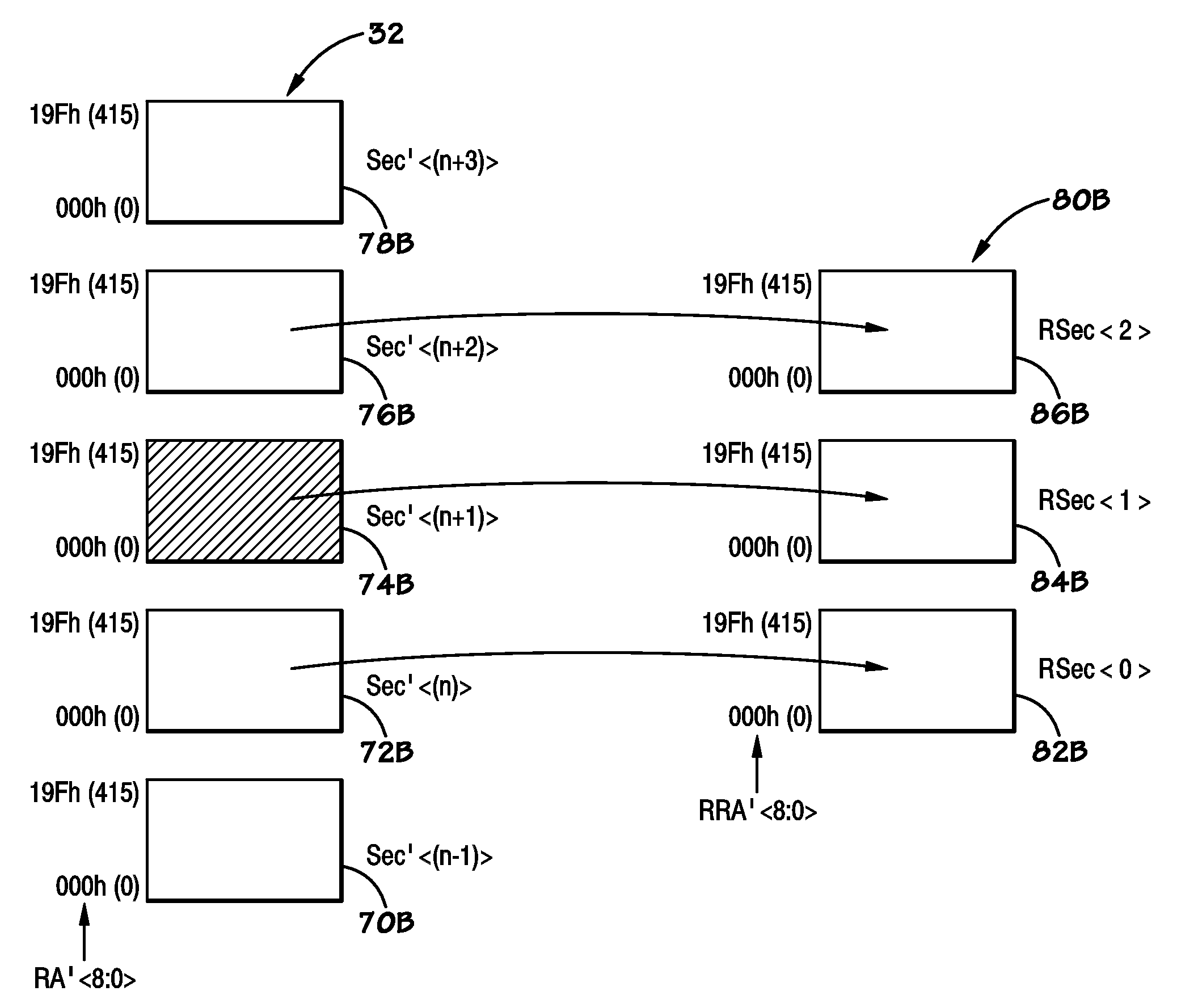
[0017]As discussed in further detail below, the disclosed systems and methods relate to a row addressing scheme for section-replacement within a memory device. More specifically, certain embodiments include a row address mapping that is configured to map an external address to an internal address that is suitable for simplified section replacement. In some embodiments, a system employing row address mapping includes a redundant row activation path having a row address converter that is configured to map an external address to an internal address (e.g., an internal row address). In some embodiments, the internal address enables simplified section replacement. In some embodiments, the row address converter is employed prior to a section replacement detector, and, in some embodiments, the row address converter is employed in parallel with a section address generator. Accordingly, embodiments that employ one or more of these techniques are believed to increase the speed of the redundant...


PUM


Abstract

Embodiments are provided that include a row decoder, including a row activation path, having a row address converter with an output coupled to an input of a section replacement detector. Further embodiments provide a method including mapping an external row address to an internal row address, wherein the internal row address comprises a section address, determining whether a section corresponding to the section address includes an error, and if the section includes an error, converting the internal row address to a redundant row address, wherein mapping the external row address to the internal row address is initiated prior to determining whether the section replacement should be performed. Further embodiments include a method for receiving a row address for a row in a memory section including a non-2^n number of normal rows and mapping the row address to a redundant row address by substracting a value from the row address.

Description

BACKGROUND[0001]1. Field of the Invention[0002]Embodiments of the invention relate generally to the field of memory devices and more particularly, to a system and method of address mapping and section replacement within a memory device.[0003]2. Description of the Related Art[0004]DRAM memory is a volatile memory that can be electrically erased and reprogrammed. DRAM memory generally stores information via an access device (e.g., an FET) and a capacitor, which are generally referred to in combination as a “cell.” Each cell traditionally stores one bit of information that is represented as a “0” or a “1”. The memory device often includes a grid-like arrangement including rows and columns of cells that are referred to as a block. Multiple blocks are combined to form a memory array. Unfortunately, not all of the cells and blocks of the memory array are usable. For example, some cells and blocks are unusable (i.e., bad) when the memory device is manufactured and / or some of the cells and ...

Claims


Application Information

Patent Timeline
Patent Type & Authority Patents(United States)
IPC IPC(8): G11C8/00G11C7/00G06F9/26G06F9/34
CPCG11C29/76
Inventor NAKANISHI, TAKUYANASU, TAKUMIFUJIWARA, YOSHINORI
Owner MICRON TECH INC