Semiconductor memory device highly integrated in direction of columns

a memory device and semiconductor technology, applied in semiconductor devices, digital storage, instruments, etc., can solve the problems of high power, low speed of data readout from memory cells and data write to memory cells, and insufficient integration of the level of integration not yet reached, so as to achieve stable readout and high integration

Inactive Publication Date: 2011-06-28
RENESAS ELECTRONICS CORP
View PDF13 Cites 17 Cited by
  • Summary
  • Abstract
  • Description
  • Claims
  • Application Information

AI Technical Summary

Benefits of technology

[0007]An object of the present invention is to provide a semiconductor memory device enabling stable readout and highly integrated in a direction of the columns.
[0009]The semiconductor memory device according to the present invention enables stable readout and high integration in a direction of the columns.

Problems solved by technology

Although the SRAM cell in Japanese Patent Laying-Open No. 2002-237539 and Japanese Patent Laying-Open No. 2002-043441 is highly integrated to a certain degree, a sufficient level of integration has not yet been reached.
The SRAM is not highly integrated particularly in a direction of the columns, so that the length of bit lines is still large, and that data readout from the memory cell and data write to the memory cell are performed at a low speed and require high power.
Further, the SRAM cell consisting of eight transistors described in Japanese Patent Laying-Open No. 2002-237539 and Japanese Patent Laying-Open No. 2002-043441 has not yet achieved sufficient stability of the readout.

Method used


Image

  • Semiconductor memory device highly integrated in direction of columns
  • Semiconductor memory device highly integrated in direction of columns
  • Semiconductor memory device highly integrated in direction of columns

Examples


first embodiment

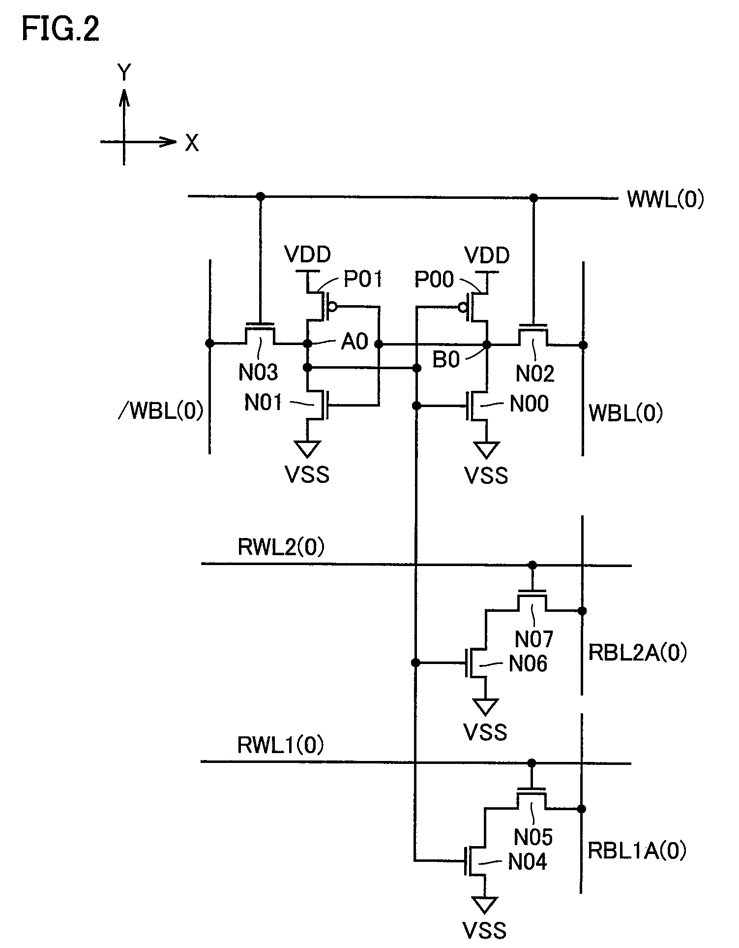
[0028]An embodiment of the present invention relates to a semiconductor memory device of a type including 10 transistors, provided with one write port and two read ports, and precharging a pair of bit lines prior to data readout from a memory cell.

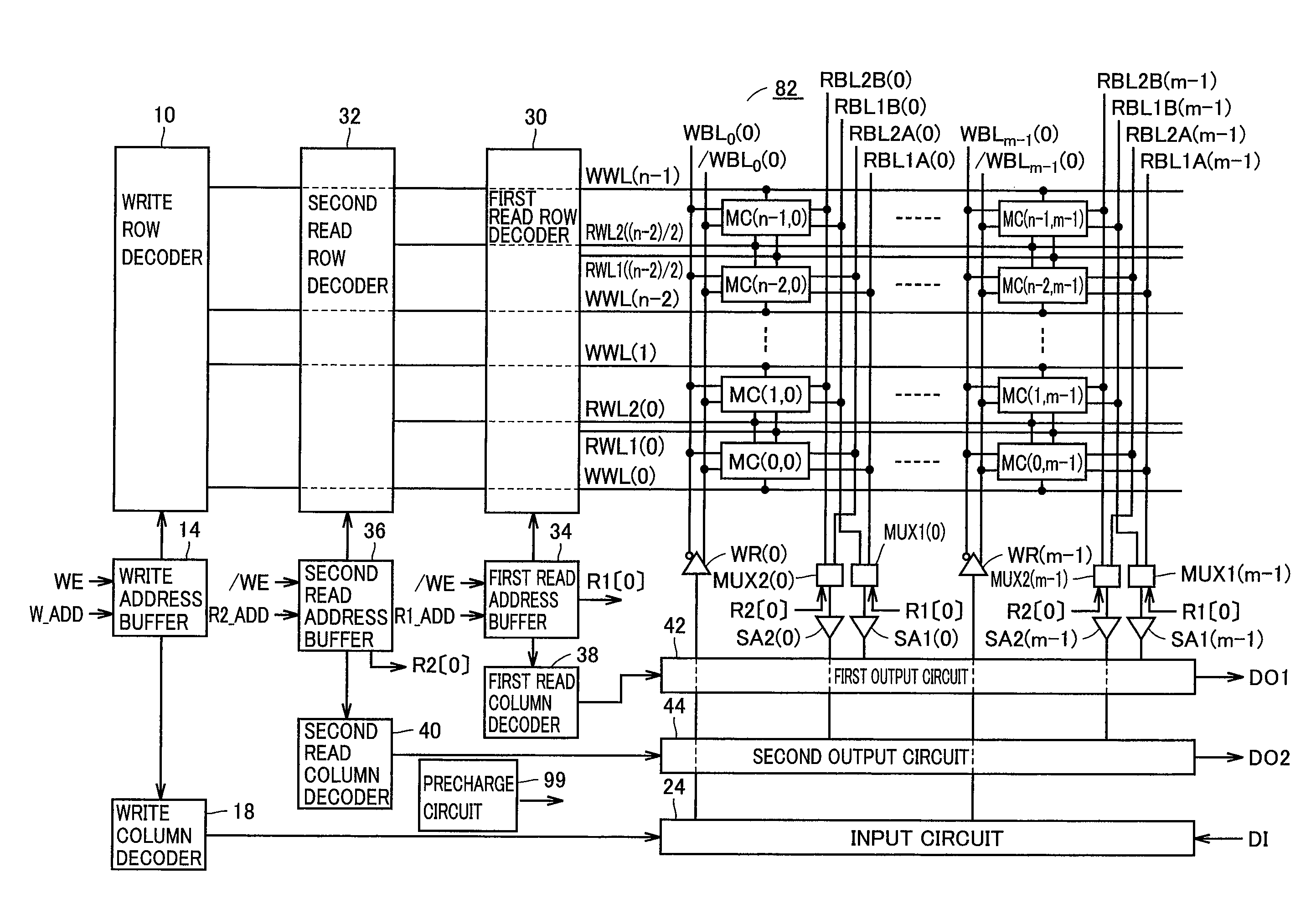
[0029]FIG. 1 is a block diagram that represents a schematic configuration of a semiconductor memory device according to a first embodiment.

[0030]With reference to FIG. 1, the semiconductor memory device includes a write address buffer 14, a first read address buffer 34, a second read address buffer 36, a write row decoder 10, a first read row decoder 30, a second read row decoder 32, a write column decoder 18, a first read column decoder 38, a second read column decoder 40, an input circuit 24, a first output circuit 42, a second output circuit 44, a memory cell array 82, and a precharge circuit 99.

[0031]Memory cell array 82 has a plurality of SRAM cells arranged in rows and columns. Given that the number of rows is n and the number of col...

second embodiment

[0113]An embodiment of the present invention relates to a semiconductor memory device of a type including 10 transistors, provided with one write port and one read port, and not precharging a pair of bit lines prior to data readout from a memory cell.

[0114]FIG. 5 is a block diagram that represents a schematic configuration of a semiconductor memory device according to a second embodiment.

[0115]With reference to FIG. 5, the semiconductor memory device includes write address buffer 14, a read address buffer 16, write row decoder 10, a read row decoder 12, write column decoder 18, a read column decoder 20, input circuit 24, an output circuit 22, and a memory cell array 84.

[0116]Memory cell array 84 has a plurality of SRAM cells arranged in rows and columns. Given that the number of rows is n and the number of columns is m, that a row closest to and a row farthest from a write driver and a sense amplifier are provided with reference numbers 0 and (n−1), respectively, and that a column c...

third embodiment

[0180]An embodiment of the present invention relates to a modification of the exemplary packaging of the memory cells (the upper and lower layers) in the second embodiment.

[0181](Exemplary Packaging of Memory Cells: Lower Layer)

[0182]FIG. 9 is a plan view that shows an arrangement of the lower layer including a well, a diffusion region, a polysilicon, a contact hole, a first-layer metal interconnection, and a first via hole of a memory cell array in a third embodiment.

[0183]As shown in FIG. 9, memory cells for two bits, namely, memory cell MC (0, 0) and memory cell MC (1, 0) adjacent thereto in the Y direction are presented. In FIG. 9, reference characters are attached only to one contact hole CT, polycrystalline silicon (polysilicon) PO, and diffusion region DF as representative examples.

[0184]In memory cells MC (0, 0) and MC (1, 0), a P-well PW301, an N-well NW301, a P-well PW302, and an N-well NW302 are formed in this order in the positive direction of the X-axis at a surface of ...


PUM


Abstract

First and second read word lines are provided in each set made of two adjacent rows. First, second, third, and fourth read bit lines are provided in each column. Each of the first and second read word lines is connected to memory cells in a corresponding one of the sets. Each of the first and third read bit lines is connected to a memory cell in one row in each of the sets, out of memory cells in a corresponding one of the columns. Each of the second and fourth read bit lines is connected to a memory cell in the other row in each of the sets, out of the memory cells in the corresponding one of the columns.

Description

BACKGROUND OF THE INVENTION[0001]1. Field of the Invention[0002]The present invention relates to a semiconductor memory device, and particularly relates to a technique of highly integrating a semiconductor memory device.[0003]2. Description of the Background Art[0004]Conventionally, there have been proposed layout structures of an SRAM (Static Random Access Memory) for high integration (e.g. see Japanese Patent Laying-Open No. 09-270468 and Japanese Patent Laying-Open No. 10-178110). An SRAM cell in these documents consists of six transistors, and thus due to variations among the transistors associated with miniaturization, data may be written to the memory cell at the time of readout via a bit line precharged to a high level, so that stable readout may not be performed.[0005]In contrast, there is disclosed a 2-port SRAM cell consisting of eight transistors (e.g. see Japanese Patent Laying-Open No. 2002-237539 and Japanese Patent Laying-Open No. 2002-043441).[0006]Although the SRAM ...

Claims


Application Information

Patent Timeline
Patent Type & Authority Patents(United States)
IPC IPC(8): G11C8/00
CPCG11C7/18G11C8/06G11C8/10H01L27/1104G11C8/16G11C11/412H01L27/0207G11C8/14H10B10/12
Inventor NII, KOJI
Owner RENESAS ELECTRONICS CORP
Why Eureka
Try Eureka