Solid-state memory device, data processing system, and data processing device

A solid-state memory, memory cell technology, applied in the direction of electric solid-state devices, semiconductor devices, electrical components, etc., can solve the problems of current path change, uneven current, inability to read data correctly, and achieve stable reading and small fluctuations. Effect

Inactive Publication Date: 2010-12-22
PS4 LUXCO SARL
View PDF6 Cites 9 Cited by
  • Summary
  • Abstract
  • Description
  • Claims
  • Application Information

AI Technical Summary

Problems solved by technology

As a result, the current flow becomes non-uniform and with each phase transition, the current path changes
Therefore, every time the phase changes, the resistance changes, which causes a problem that the data cannot be read correctly

Method used


Image

  • Solid-state memory device, data processing system, and data processing device
  • Solid-state memory device, data processing system, and data processing device
  • Solid-state memory device, data processing system, and data processing device

Examples


Embodiment Construction

[0057] Hereinafter, preferred embodiments of the present invention will be described in detail with reference to the accompanying drawings.

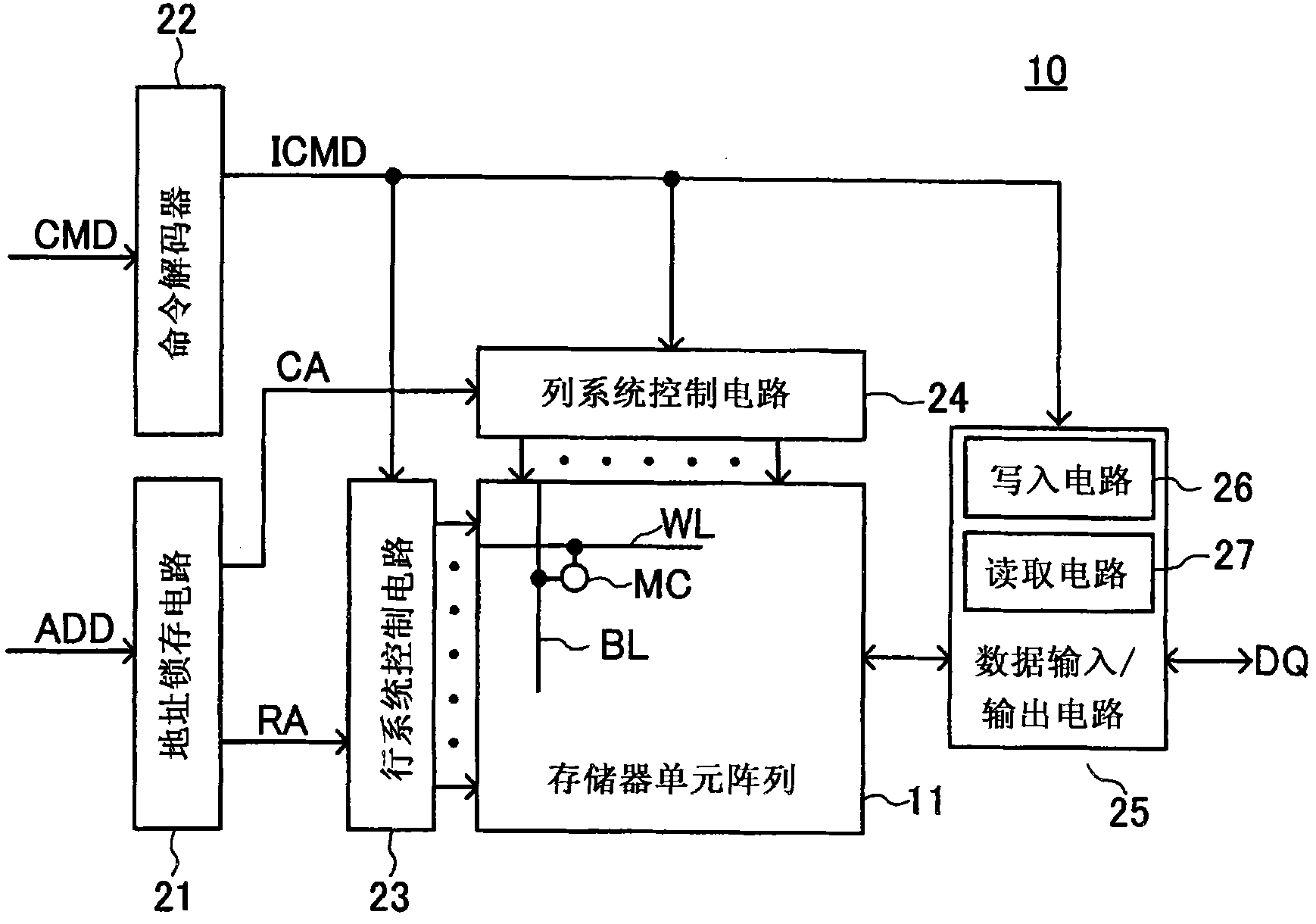
[0058] figure 1 is a block diagram of a semiconductor memory 10 according to an embodiment of the present invention.

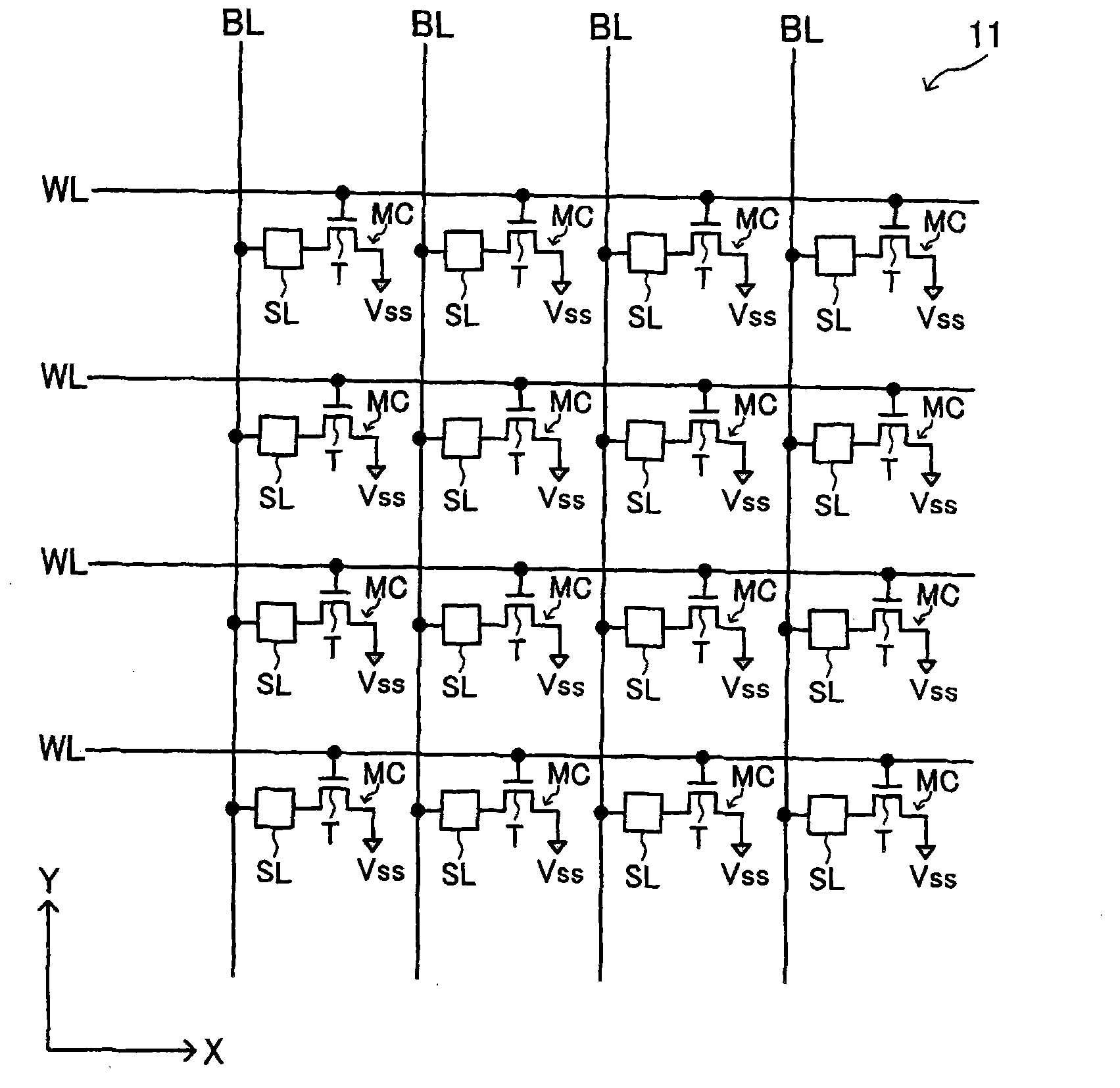
[0059] The semiconductor memory 10 according to the present embodiment is a PRAM, and can access a memory cell array 11 including many memory cells MC by inputting an address signal ADD and a command CMD from the outside. That is, when the command CMD indicates a read operation, the data held in the memory cell MC designated by the address signal ADD is read out. When the command CMD indicates a write operation, write data input from the outside is written in the memory cell MC designated by the address signal ADD.

[0060] Below are more specific instructions. The semiconductor memory 10 has an address latch circuit 21 that holds an address signal ADD, and a command decoder 22 that generates an internal command ICMD ...


PUM


Abstract

The invention provides a solid-state memory device, a data processing system and a data processing device. The solid-state memory device includes: a superlattice laminate having plural crystal layers laminated therein, the crystal layers including first and second crystal layers having mutually opposite compositions; a lower electrode provided on a first surface in a laminating direction of the superlattice laminate; and an upper electrode provided on a second surface of the superlattice laminate in the laminating direction. The first crystal layer included in the superlattice laminate is made of a phase change compound. According to the present invention, the superlattice laminate laminated in opposite directions of the upper and lower electrodes is sandwiched between these electrodes. Therefore, when an electric energy is applied to the superlattice laminate via these electrodes, a uniform electric energy can be applied to a laminated surface of the superlattice laminate. Accordingly, fluctuation of a resistance is small even when information is repeatedly rewritten, and data can be read stably as a result.

Description

technical field [0001] The present invention relates to solid-state memory, and more particularly, to solid-state memory using superlattice devices. The invention also relates to a data processing system and a data processing device comprising such a solid state memory. Background technique [0002] In recent years, a semiconductor memory called PRAM (Phase Change Random Access Memory) has attracted attention. The PRAM is a semiconductor memory that uses a phase-change material as a material of a recording layer, and records information therein by using a difference between resistance in a crystalline phase and resistance in an amorphous phase. [0003] Specifically, when a chalcogenide is used as a phase change compound, the resistance becomes relatively low in the crystalline phase, and the resistance becomes relatively high in the amorphous phase. Therefore, when the resistance of the phase change compound is detected by flowing a read current, stored data can be read o...

Claims


Application Information

Patent Timeline
Patent Type & Authority Applications(China)
IPC IPC(8): H01L45/00
CPCH01L27/2409H01L45/1675H01L27/2454H01L45/065H01L45/144H01L45/1683H01L45/126H01L45/1616H01L45/1625H01L45/1233H10B63/34H10B63/20H10N70/235H10N70/8413H10N70/023H10N70/026H10N70/066H10N70/8828H10N70/063H10N70/826H10N70/8825
Inventor 相泽一雄浅野勇富永淳二吾历钻汰·来露保富步尾瑠·本须路破人·新富尊
Owner PS4 LUXCO SARL
Why Eureka
Try Eureka