Input sensor containing display device and method for driving the same

a display device and input sensor technology, applied in the field of planar display devices, can solve problems such as inability to reliably detect, read speed may create a problem, and marked differences in characteristics (or detection capability) between amplifiers, and achieve the effect of flexible data processing and efficient display data processing

Active Publication Date: 2009-11-03
JAPAN DISPLAY CENTRAL CO LTD
View PDF19 Cites 11 Cited by
  • Summary
  • Abstract
  • Description
  • Claims
  • Application Information

AI Technical Summary

Benefits of technology

[0012]Thus, according to an aspect of the present invention, there is provided a display device containing an input sensor (for example, a photoelectric conversion element), which device can flexibly process data and which has various applications, the device being able to efficiently process display data, read data, and data on associations between the display data and image pickup data.
[0013]According to another aspect of the present invention, there is provided a display device containing an input sensor (for example, a photoelectric conversion element), which device can improve a data read speed.
[0014]According to another aspect of the present invention, it is possible to avoid making the results of detections unstable particularly as a result of differences in characteristics between amplifiers that obtain optical sensor outputs, thus accomplishing stable reads. Further, a method for driving an input device containing display device is provided, which method is implemented by effectively utilizing signal lines inherently used to input display signals and without the need to increase the number of components.
[0017]As described above, the display device has the read signal processing means for processing the sense signal output by the read circuit in accordance with a command requesting execution of an application and the interface section which transfers a command requesting execution of the application to the read signal processing means. Consequently, various processes can be executed to improve flexibility.
[0019]The sense signals output by the read circuit are arithmetic outputs of sense signals from the plurality of optical sensors. This sharply increases the read speed compared to that in which a sense signal is read from each optical sensor.

Problems solved by technology

Further, if data is to be read from the photoelectric conversion element, its read speed may create a problem.
However, in the display device, since TFT amplifiers are constructed on the glass substrate, there are marked differences in characteristics (or detection capability) between amplifiers.
With such marked differences in characteristics between the amplifiers, the results of detections are not reliable.
This may cause the results of detections to be incorrectly recognized.
Therefore, the reliability of the product may be degraded.

Method used


Image

  • Input sensor containing display device and method for driving the same
  • Input sensor containing display device and method for driving the same
  • Input sensor containing display device and method for driving the same

Examples


second embodiment

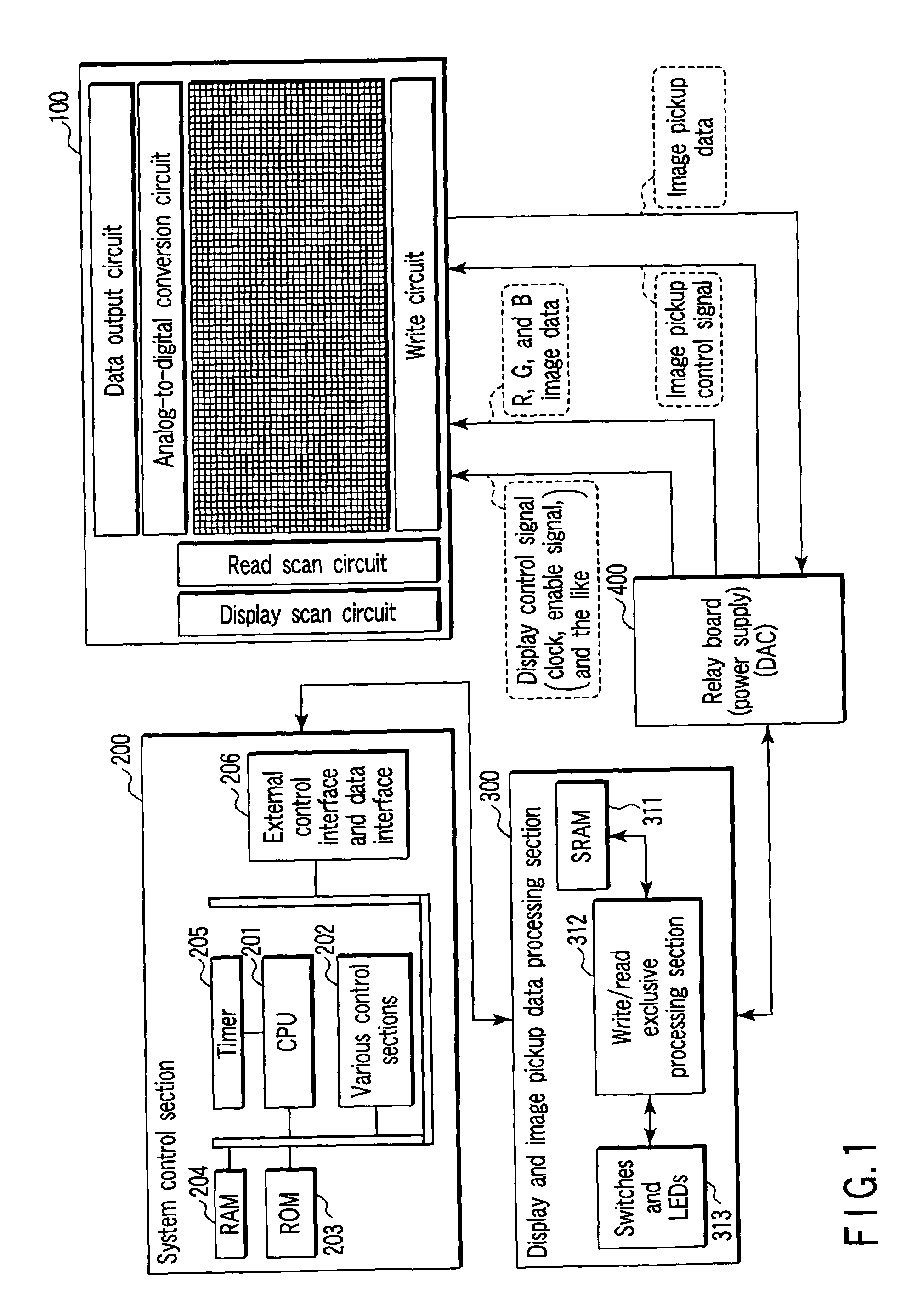
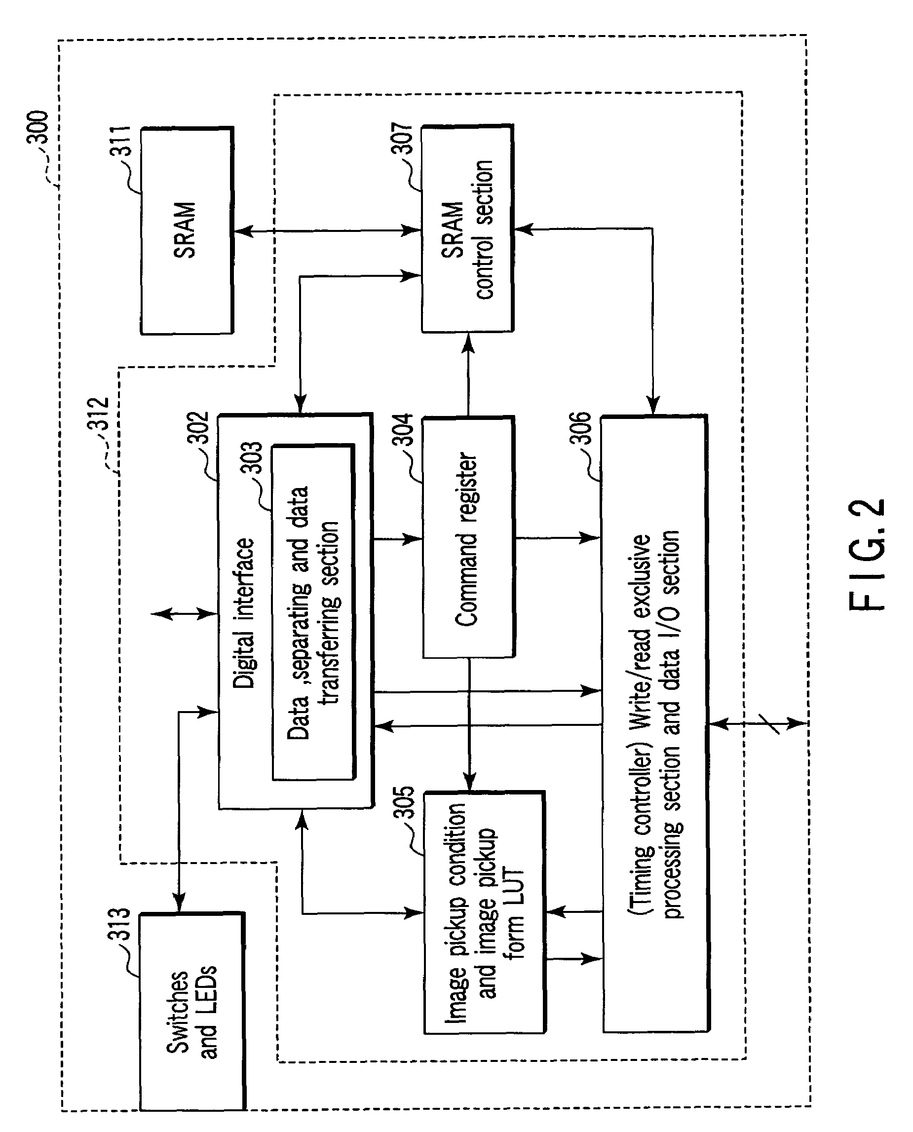
According to Image Pickup System

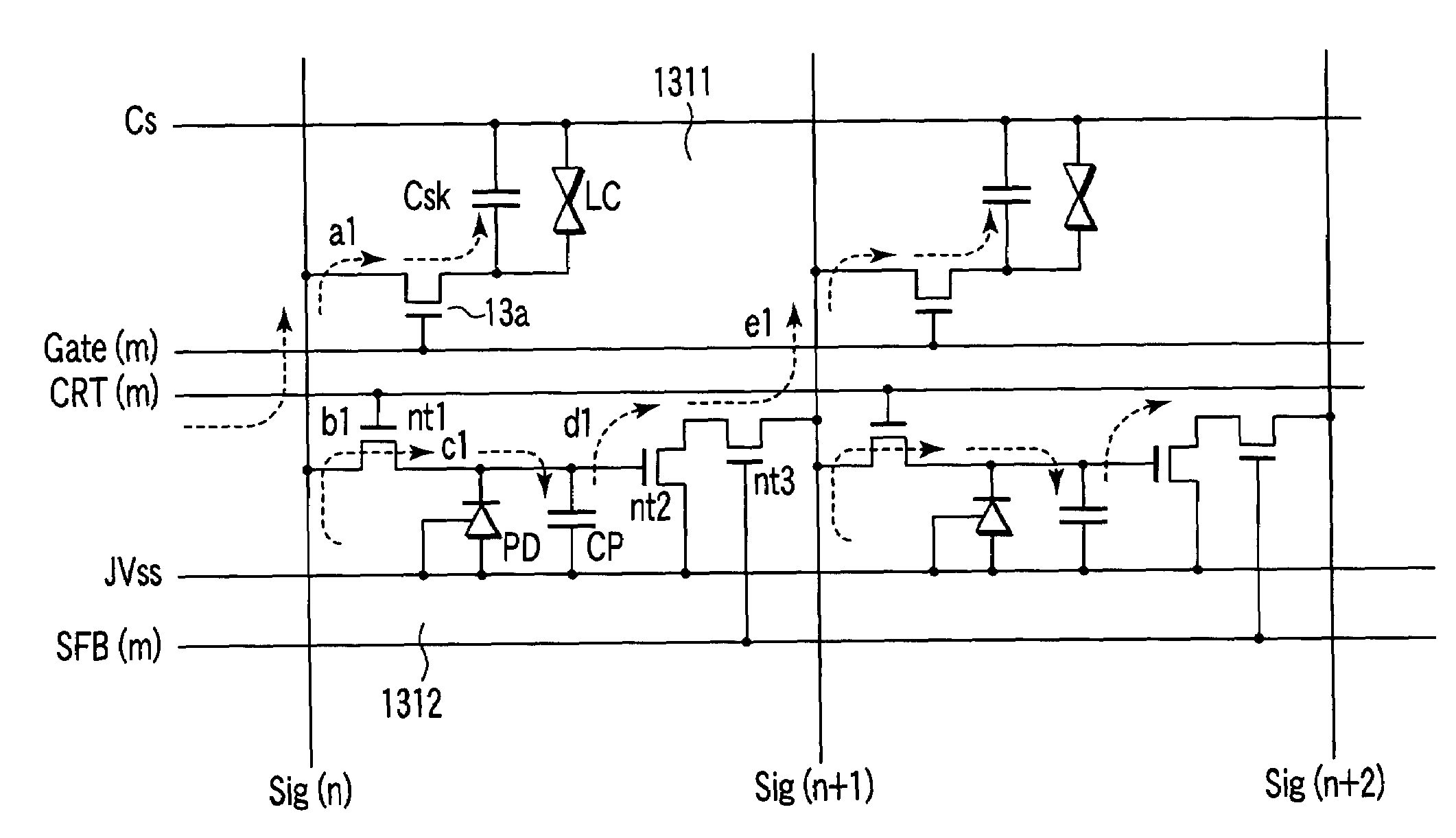
[0107]A second embodiment is characterized in that the precharge voltage of the sensor capacitor CP is varied with the sensors on the basis of the results of calibration image pickup. In the calibration image pickup, light from the backlight is, for example, uniformly applied. In this case, even within the same chip, there may be noticeable differences among the optical sensors (photodiodes) PD or transistors nt2 formed on the glass substrate. Thus, disadvantageously, some parts of the image may appropriately show reflected light from an indicating member such as a finger in white while showing the absence of reflected light in black, but other parts may undergo underexposure or overexposure to prevent the indicating section from being properly detected. This is due to differences among the currents through the optical sensors or differences among the thresholds of the transistors nt2. In this case, the underexposure or overexposure is avoided by incr...


PUM

PropertyMeasurementUnit
precharge voltagesaaaaaaaaaa
voltageaaaaaaaaaa
voltageaaaaaaaaaa

Abstract

An input sensor containing a display device including a group of pixel circuits arranged in a matrix, a group of optical sensor circuits arranged in a matrix, a display driving circuit which provides a display signal to the display element group and which provides a driving signal to the display element group, a read circuit which identifies an optical sensor to read a sense signal from this optical sensor, and a read signal processing section which processes the sense signal output by the read circuit in accordance with a command. The read signal processing section has an interface section which transfers, when the command requesting execution of an application is set to the interface section, the command to a command register.

Description

CROSS-REFERENCE TO RELATED APPLICATIONS[0001]This application is based upon and claims the benefit of priority from prior Japanese Patent Applications No. 2004-096829, filed Mar. 29, 2004; No. 2004-144950, filed May 14, 2004; and No. 2004-144951, filed May 14, 2004, the entire contents of all of which are incorporated herein by reference.BACKGROUND OF THE INVENTION[0002]1. Field of the Invention[0003]The present invention relates to a planar display device using liquid crystal or light emitting elements, and in particular, to an input sensor containing display device that contains input sensors.[0004]2. Description of the Related Art[0005]A liquid crystal display device comprises an array substrate on which signal lines, scan lines, and pixel transistors (for example, thin film transistors) are provided in a line and a driving circuit that drives the signal lines and the scan lines. Recent progress and development of integrated circuit technologies have put to practical use a proces...

Claims


Application Information

Patent Timeline
Patent Type & Authority Patents(United States)
IPC IPC(8): H04N3/14G09G3/36H01L31/00H04N5/335G02F1/133G06F3/041H04N5/225
CPCG06F3/0412G02F1/13338G06F3/042G09G3/20G09G3/36
Inventor NAKAMURA, TAKASHIYOSHIDA, MASAHIROHAYASHI, HIROTAKA
Owner JAPAN DISPLAY CENTRAL CO LTD
Why Eureka
Try Eureka