

Stack having Heusler alloy, magnetoresistive element and spin transistor using the stack, and method of manufacturing the same
a technology of magnetoresistive elements and stacks, which is applied in the direction of solid-state devices, magnetic bodies, transportation and packaging, etc., can solve the problems of low degree of freedom of selection of underlying layers, inability to extract high-performance devices using heusler alloys, and inability to achieve high-performance devices
- Summary
- Abstract
- Description
- Claims
- Application Information
AI Technical Summary
Problems solved by technology
Method used
Image

Examples
first embodiment
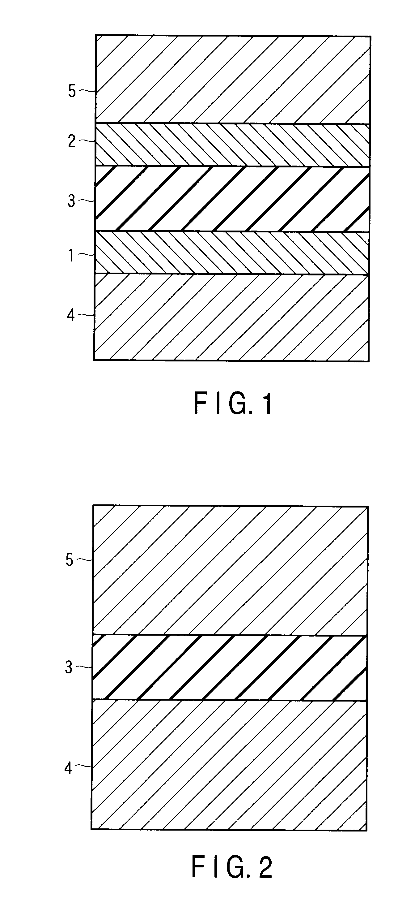
[0036]First, a stack of the first embodiment of the present invention and a magnetoresistive element including the stack will be explained below.
[0037]FIG. 1 is a sectional view showing the structure of the magnetoresistive element including the stack of the first embodiment.
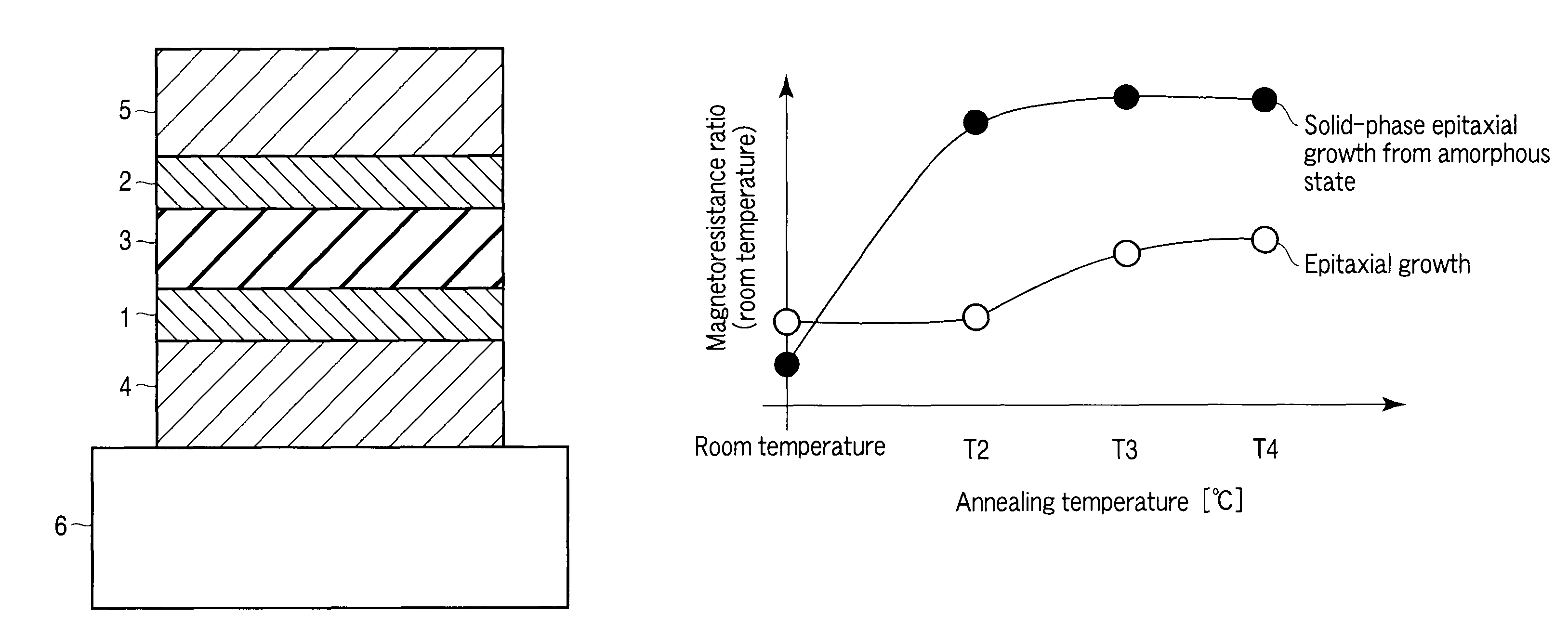
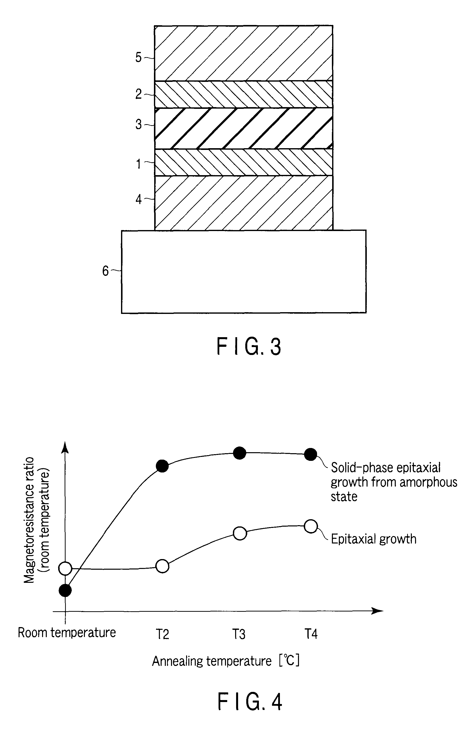
[0038]As shown in FIG. 1, the stack has a crystalline MgO layer 3, a crystalline Heusler alloy layer 1 formed in contact with the MgO layer 3, and an amorphous Heusler alloy layer 4 formed on that surface of the Heusler alloy layer 1, which is opposite to the surface on which the MgO layer 3 is formed. “Crystalline” includes a single crystal and polycrystal. The “crystal orientation” of a polycrystal indicates the crystal orientation in a crystal grain.
[0039]The magnetoresistive element including the above-mentioned stack is formed as follows. The crystalline MgO layer 3 is formed between the crystalline Heusler alloy layer 1 and a crystalline Heusler alloy layer 2. The amorphous Heusler alloy layer 4 is formed ...
second embodiment
[0067]A spin MOSFET of the second embodiment of the present invention will be explained below.
[0068]FIG. 5 is a sectional view showing the structure of the spin MOSFET of the second embodiment.
[0069]As shown in FIG. 5, impurity diffusion layers 10A as a source and drain are formed in the surface region of a semiconductor substrate 10 by ion implantation. MgO layers 11 are formed on the impurity diffusion layers 10A. Crystalline Heusler alloy layers 12 are formed on the MgO layers 11, and amorphous Heusler alloy layers 13 are formed on the Heusler alloy layers 12. In addition, a gate insulating film 14 is formed on the semiconductor substrate 10 between the source and drain, and a gate electrode 15 is formed on the gate insulating film 14. Note that the impurity diffusion layers 10A may also be omitted. Note also that the stacked structure of the MgO layer 11 and Heusler alloy layers 12 and 13 may also be formed on only one of the source and drain.
[0070]The MgO layer 11 is a tunnel b...
third embodiment
[0083]A magnetoresistive element of the third embodiment of the present invention will be explained below.
[0084]FIG. 6 is a sectional view showing the structure of the magnetoresistive element of the third embodiment. The magnetoresistive element of the third embodiment includes a double-junction structure (double junction) having two MgO layers as tunnel barrier layers.
[0085]A stacked structure in which a crystalline MgO layer 3, Heusler alloy layer 7, and crystalline MgO layer 8 are stacked in this order is formed between crystalline Heusler alloy layers 1 and 2. An amorphous Heusler alloy layer 4 is formed on that surface of the Heusler alloy layer 1, which is opposite to the surface on which the MgO layer 3 is formed. In addition, an amorphous Heusler alloy layer 5 is formed on that surface of the Heusler alloy layer 2, which is opposite to the surface on which the MgO layer 8 is formed. The magnetoresistive element having this structure is formed on a silicon semiconductor subs...
PUM
| Property | Measurement | Unit |
|---|---|---|
| thickness | aaaaa | aaaaa |
| temperature | aaaaa | aaaaa |
| thickness | aaaaa | aaaaa |
Abstract
Description
Claims
Application Information