Method of detecting and passivating a defect in a solar cell

a solar cell and defect technology, applied in the field of solar cell defect detection and passivating, can solve the problems of high defectivity of devices, high cost of electricity generated by silicon-based solar cells, and inadvertent introduction of defects into the device structure, so as to reduce the defect rate and improve the efficiency of the thin film solar cell. , the effect of detecting efficiency

Inactive Publication Date: 2011-07-19
SOLOPOWER
View PDF17 Cites 13 Cited by
  • Summary
  • Abstract
  • Description
  • Claims
  • Application Information

AI Technical Summary

Benefits of technology

[0013]The present inventions relate to method and apparatus for detecting efficiency reducing defects in a thin film solar cell such as a Group IBIIIAVIA compound thin film solar cell, and cutting a section of the solar cell to improve its efficiency.

Problems solved by technology

However, the cost of electricity generated using silicon-based solar cells is higher than the cost of electricity generated by the more traditional methods.
A common practical problem associated with manufacturing thin film devices, however, is the inadvertent introduction of defects into the device structure.
Since the total thickness of the electrically active layers of thin film solar cells is in the range of 0.5-5 micrometers, these devices are highly sensitive to defectivity.
There may be different types of defects in thin film solar cell structures.
Some of these defects may be only morphological in nature and they may be “nuisance defects”, which are not electrically active.
Other defects, on the other hand, may be electrically active and may negatively impact the performance of the device.
Shunting defects, for example, may introduce a shunting path through which the electrical current of the device may leak through and therefore they may be considered to be “killer defects”.
However, etching or anodizing of CIGS type compound materials leave behind conductive residues comprising metallic species of Cu, In or Ga at the etched location that actually may make shorting even worse than before etching.
This approach may work for thick crystalline solar cells, but would damage thin film devices.
Again such an approach is not applicable to flexible thin film devices such as CIGS cells, because as will be discussed later, defects in such thin film structures need to be detected and fixed before the solar cell is actually completed.
Therefore, one defect removal method which may work for one device may not work for the other.
For CIGS, there is to date no successful laser ablation process because laser heating of this compound semiconductor leaves behind conductive phases comprising Cu, In, Ga metals and / or Cu—Se phases.
Similarly, techniques using chemical etching of defect areas introduce problems for devices employing compound semiconductors such as CdTe and CIGS(S).
In such compounds, chemical etching does not etch the material uniformly and leaves behind conductive residue.
In such thin and flexible device structures scribing over the defect with a mechanical tool peels off and damages the various device layers at the vicinity of the defect which already has a shorting path for the electrical current, and also damages the metallic substrate which is flexible and pliable.
Such damage from the conducting parts of the solar cell may create conductive debris shorting the top surface of the device to the substrate, the debris originating from the damaged substrate region, the contact layer as well as the transparent conductive layer and especially the portion of the grid pattern damaged by the scribing tool.
Laser approaches used to remove defects from standard solar cells also do not work well for foil based thin film devices such as CIGS type devices.
First of all, adjustment of the laser power to remove only the top transparent conductive layer or the grid pattern at the defect region is very difficult, and sometimes impossible.
The laser beam, by heating the grid pattern and / or the metallic substrate, may cause local melting of the metal substrate and cause new shorting defects, especially for thin film solar cell structures constructed on conductive substrates.
Such conductive debris is a source of new shorting defects in the device structure.
Especially the most serious shorting defects which are under the grid pattern may not be removed by laser processes.

Method used


Image

  • Method of detecting and passivating a defect in a solar cell
  • Method of detecting and passivating a defect in a solar cell
  • Method of detecting and passivating a defect in a solar cell

Examples


Embodiment Construction

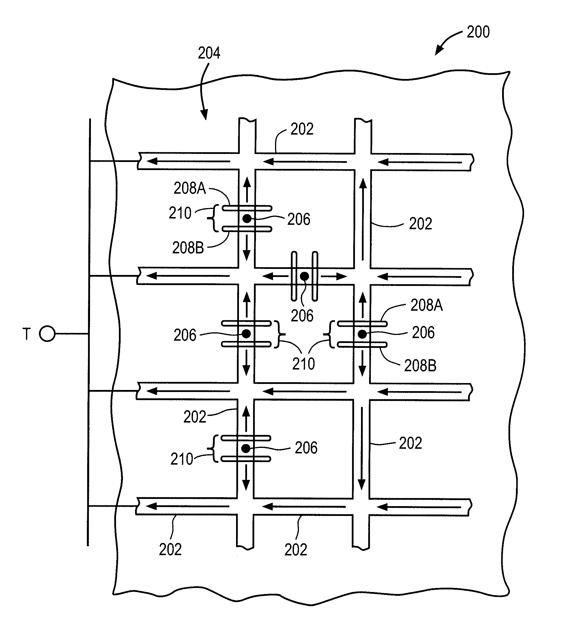
[0032]The embodiments of the present inventions provide defect detection processes, apparatus to detect defects in solar cell structures and methods and apparatus to passivate that defect. In some embodiments, instead of passivating or removing the defect itself, its effect is reduced or eliminated by partially cutting the solar cell structure including the substrate, in predetermined locations. These methods are especially suited for flexible thin film solar cell structures built on flexible thin film substrates such as polymeric substrates and metallic substrates. Such polymeric substrates include, but are not limited to polyimide-based high temperature substrates, and the metallic substrates include but are not limited to stainless steel, titanium, molybdenum, and aluminum containing conductive substrates. The semiconductor absorber layers of such flexible substrates may include CIGS type materials, cadmium telluride type Group II-VI materials, amorphous Si, polycrystalline or mi...


PUM

PropertyMeasurementUnit
total thicknessaaaaaaaaaa
thicknessaaaaaaaaaa
thicknessaaaaaaaaaa

Abstract

The present invention provides methods of manufacturing a high efficiency solar cell. In one embodiment, in a solar cell having a grid pattern that channels current, a defect causes an undesired current flow is removed by mechanically removing a portion of the grid pattern, thereby passivating the defect by removing a segment of the solar cell adjacent the defect. The segment also includes the front and back portions of the solar cell at the location of the defect without including the defect.

Description

CROSS REFERENCE TO RELATED APPLICATIONS[0001]This application claims priority to U.S. Provisional Patent Application No. 61 / 154,324 filed Feb. 20, 2009 and this application claims priority to and is a continuation in part of U.S. patent application Ser. No. 12 / 703,120 filed Feb. 9, 2010, and this application is a continuation-in-part of U.S. patent application Ser. No. 12 / 272,499 filed Nov. 17, 2008, all of which are incorporated by reference.BACKGROUND[0002]1. Field of the Inventions[0003]The present inventions relate to method and apparatus for detecting the locations of shorting defects in a thin film solar cell such as in Group IBIIIAVIA compound thin film solar cells fabricated on flexible foil substrates, and reducing the effect of such defects on the device by cutting a carefully selected section of the solar cell.[0004]2. Description of the Related Art[0005]Solar cells are photovoltaic devices that convert sunlight directly into electrical power. The most common solar cell m...

Claims


Application Information

Patent Timeline
Patent Type & Authority Patents(United States)
IPC IPC(8): B23P6/00
CPCH01L31/03928H01L31/0749H01L31/18H01L31/186H01L31/046G01N21/9501G01R31/025Y10T29/49117H02S50/10Y10T29/4913Y10T29/49155Y10T29/49721Y10T29/49726Y02E10/541G01R31/52Y02P70/50
Inventor BASOL, BULENT M.
Owner SOLOPOWER
Why Eureka
Try Eureka