Sample observing method and scanning electron microscope

a scanning electron microscope and sample technology, applied in the direction of material analysis using wave/particle radiation, instruments, nuclear engineering, etc., can solve the problems of lowering the efficiency of secondary electron detection and difficult to extract the pattern profile, and achieve the effect of minimizing the effect of throughput and high accuracy

Active Publication Date: 2011-12-15
HITACHI HIGH-TECH CORP
View PDF11 Cites 8 Cited by
  • Summary
  • Abstract
  • Description
  • Claims
  • Application Information

AI Technical Summary

Benefits of technology

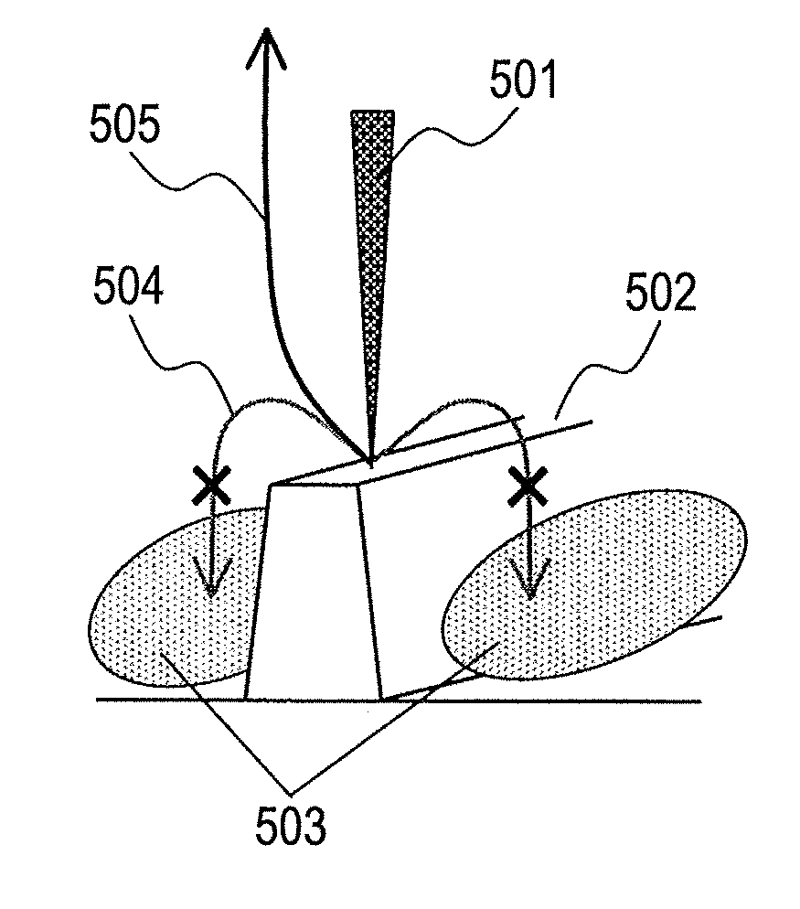
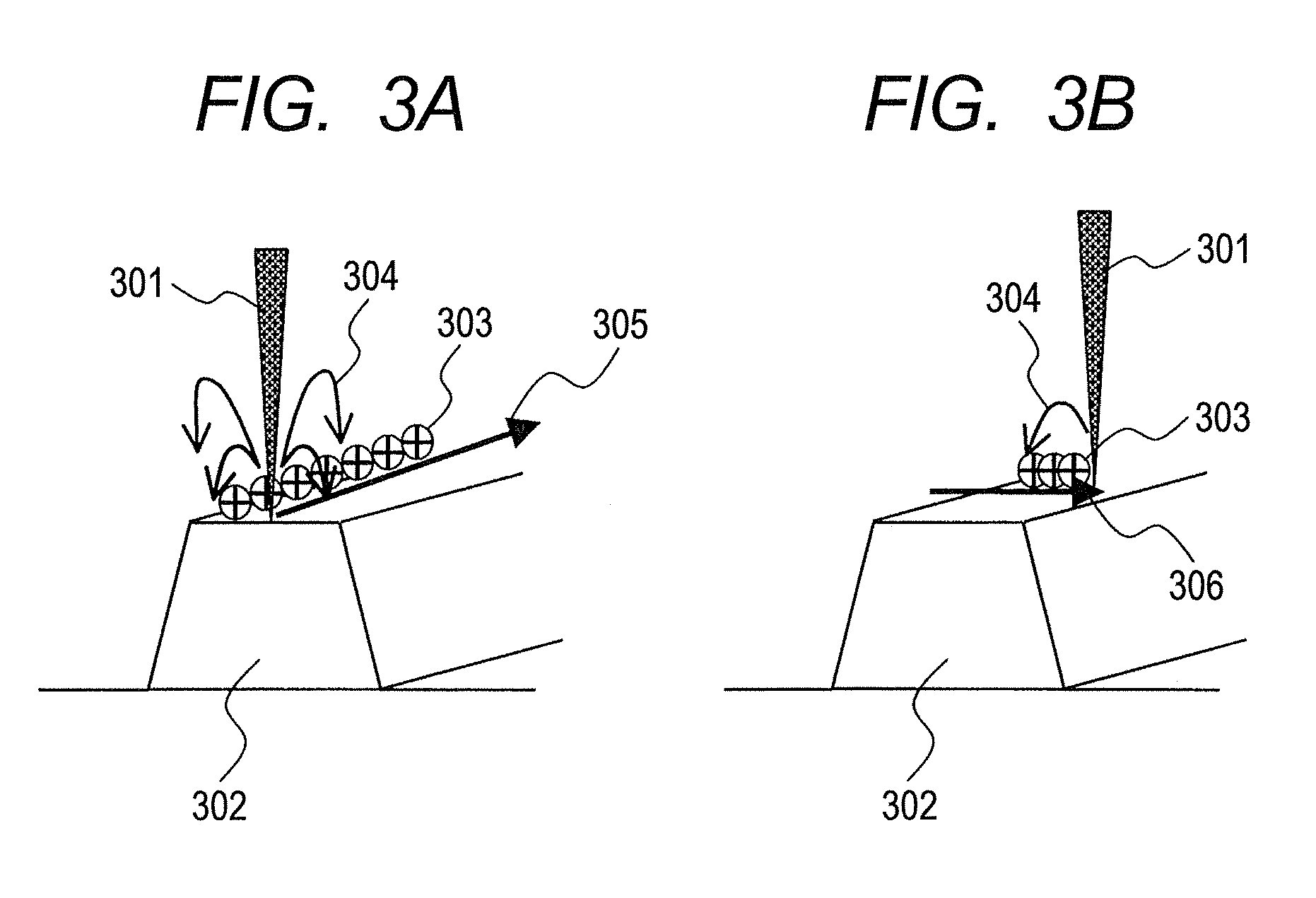
[0007]FIG. 3A illustrates the electron beam scanning in the parallel direction 305 with respect to the insulator pattern 302. In this case, the positive charge 303 on the sample surface is intensified because of continuous scanning with respect to the insulator portion so that the secondary electron 304 generated by the electron beam irradiation tends to be returned to the sample surface. As a result, secondary electron detection efficiency is lowered, which makes it difficult to extract the pattern profile.
[0011]Japanese Patent Application Laid-Open Publication No. 2008-123716 discloses the technology which discriminates the secondary electron energy using the energy filter, measures fluctuation in the sample potential based on the change in the obtained electron yield, extracts time constant of charge formed upon electron beam irradiation, optimizes the interlace scanning interval based on the extracted time constant, and suppresses strain which appears on the SEM image and magnification fluctuation. This method is expected to provide the effect with respect to the aforementioned task to a certain level. However, it is predicted to make it difficult to optimize the scanning interval conforming to the LSI pattern shape expected to be further complicated in future.
[0013]It is an object of the present invention to provide a sample observing method for obtaining the pattern profile with high accuracy even in a complicated LSI pattern, regardless of the electron beam scanning direction while minimizing the effect on the throughput.
[0014]It is another object of the present invention to provide a sample observing method with less pattern damage when observing the resist pattern.
[0016]The present invention is capable of providing the sample observing method which allows capture of the pattern profile with high accuracy even in the complicated LSI pattern, regardless of the electron beam scanning direction while minimizing the effect on the throughput.

Problems solved by technology

As a result, secondary electron detection efficiency is lowered, which makes it difficult to extract the pattern profile.

Method used


Image

  • Sample observing method and scanning electron microscope
  • Sample observing method and scanning electron microscope
  • Sample observing method and scanning electron microscope

Examples


example 1

[0045]Example 1 will be described referring to FIGS. 7A, 7B and 7C. The description that will not be explained herein is the same as the one which has been explained in the aforementioned [Principle of charge control][Device structure].

[0046]In this example, a resist pattern is used as the observation object. A line width and a film thickness of the resist pattern to be observed are set to 100 nm and 150 nm, respectively. FIG. 7A is a flowchart representing a specific procedure of the sample observation method according to the example.

[0047]The wafer is loaded in a sample chamber of the SEM (S701-1), and the stage is moved to an image capturing position (S701-2). Then a pattern layout judgment function 426 (see FIG. 4) is enabled to judge whether or not the pattern edge in parallel with the electron beam scanning direction is contained by using shape information of the observation pattern in the product design information (S702).

[0048]If it is judged that the relevant pattern edge i...

example 2

[0056]Example 2 will be described referring to FIGS. 8A, 8B and 8C. The description that will not be explained herein is the same as the one which has been explained in the aforementioned [Principle of charge control][Device structure], and Example 1.

[0057]In this example, a resist pattern is used as the observation object. A line width and a film thickness of the observation resist pattern are set to 100 nm and 150 nm, respectively. FIG. 8A is a flowchart representing a specific procedure of the sample observation method according to the example.

[0058]Likewise Example 1, the wafer is loaded in the sample chamber of the SEM (S801-1), and stage is moved to the image capturing position (S801-2). The condition other than the frame integrated number is set in accordance with the final image capturing condition, and the image of the observation pattern is captured using the frame integrated number smaller than the one for the scanning (S802). The frame integrated number smaller than the ...


PUM

PropertyMeasurementUnit
thicknessaaaaaaaaaa
thicknessaaaaaaaaaa
widthaaaaaaaaaa

Abstract

Provided is a sample observing method wherein the effect on throughput is minimized, and a pattern profile can be obtained at high accuracy even in a complicated LSI pattern, regardless of the scanning direction of an electron beam. In the sample observing method, the presence or absence of an edge parallel to a scanning direction (707) of an electron beam is judged regarding an edge (708) of a pattern to be observed (S702); if the edge is present, an area in the vicinity of the pattern edge is designated as a local pre-dose area (709) (S703); a local pre-dose of an electron beam is performed, so that the initial charged state is controlled not to return secondary electrons generated by irradiation of an electron beam when an image is captured, to the surface of a sample.

Description

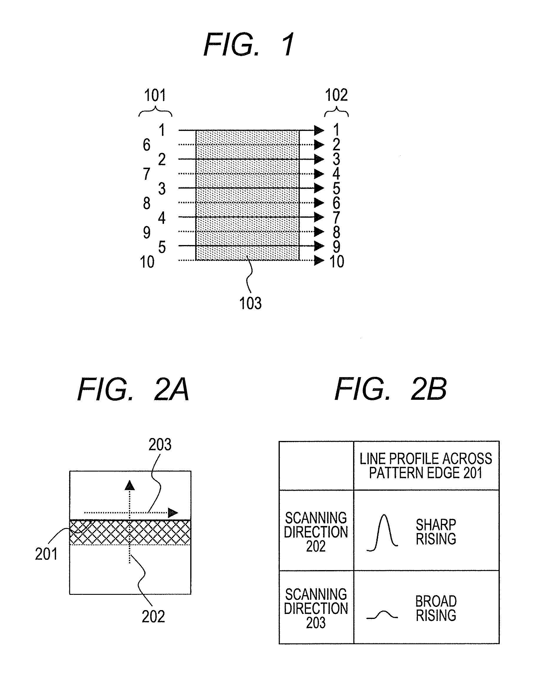
TECHNICAL FIELD[0001]The present invention relates to a sample observing method using a scanning electron microscope.BACKGROUND[0002]When observing a sample (wafer having an LSI pattern formed thereon) using an electron beam applied device, for example, scanning electron microscope (SEM: Scanning Electron Microscope), electron beams emitted from an electron gun are deflected by a scanning deflector so that a secondary electron, reflecting electron and backscatter electron generated from the sample surface are detected by electron beam scanning. The resultant signal is processed to capture an image.[0003]FIG. 1 shows a generally employed scanning (hereinafter referred to as interlace scanning). A reference numeral 101 denotes a scanning order, 102 denotes a scanning line number, and 103 denotes a scanning area. In the generally employed image display process, a secondary electron signal obtained at a scanning position on the sample is transferred to an element (pixel) for image displ...

Claims


Application Information

Patent Timeline
Patent Type & Authority Applications(United States)
IPC IPC(8): G01N23/04H01J37/28
CPCG01B15/04H01J37/222H01J2237/2817H01J2237/24592H01J37/28
Inventor OMORI, SEIKOCHENG, ZHAOHUIKAZUMI, HIDEYUKI
Owner HITACHI HIGH-TECH CORP
Why Eureka
Try Eureka