Light emitting diode package

a technology of light-emitting diodes and packages, which is applied in the direction of solid-state devices, manufacturing tools, and solvents, etc., can solve the problems of easy deformation and breakage of components, limited application of leds, and led heights smaller than 200 micrometers, so as to reduce the height of the entire assembly

Inactive Publication Date: 2011-07-19
EVERLIGHT ELECTRONICS
View PDF26 Cites 0 Cited by
  • Summary
  • Abstract
  • Description
  • Claims
  • Application Information

AI Technical Summary

Benefits of technology

[0009]An object of the present invention is to provide an improved LED to reduce the entire assembly height when the LED is mounted on a substrate.
[0010]Another object of the present invention is to provide an improved LED to eliminate the thin LED being easily damaged during transportation or storage and increase the manufacturing quality.
[0014]The LEDs in accordance with the present invention has several advantages.
[0015]First, the base apparatus provides a batch production capability for the LEDs. The LEDs can be manufactured in mass production to decrease cost. Further, the LEDs can be mounted on a substrate by its sides so that its entire assembly height is reduced when the LEDs are mounted on the substrate. Therefore, thin and weak components (such as thin substrate or leadframe) of the LEDs do not need to be used, eliminating damage to the components during transportation or storage. The cost of the LED is decreased, and the manufacturing quality of the LED is improved.
[0016]In addition, since the illuminating devices are mounted on the fingers in the vertical direction relative to the base apparatus, the current machining apparatus can be used without any modifications. Therefore, the present invention is easy to operate and use.

Problems solved by technology

To manufacture an LED with a height smaller than 200 micrometers is difficult, and results in limited applications of the LED.
However, to thin down the components weakens the component's stiffness, which causes the component to be easily deformed and broken during manufacturing processes.
Therefore, the thinned components may be difficult to transport and store because the probability of being damaged during transportation and storage is raised, as well as manufacturing cost.

Method used


Image

  • Light emitting diode package
  • Light emitting diode package
  • Light emitting diode package

Examples


Embodiment Construction

[0025]Reference will now be made in detail to the present preferred embodiments of the invention, examples of which are illustrated in the accompanying drawings. Wherever possible, the same reference numbers are used in the drawings and the description to refer to the same or like parts.

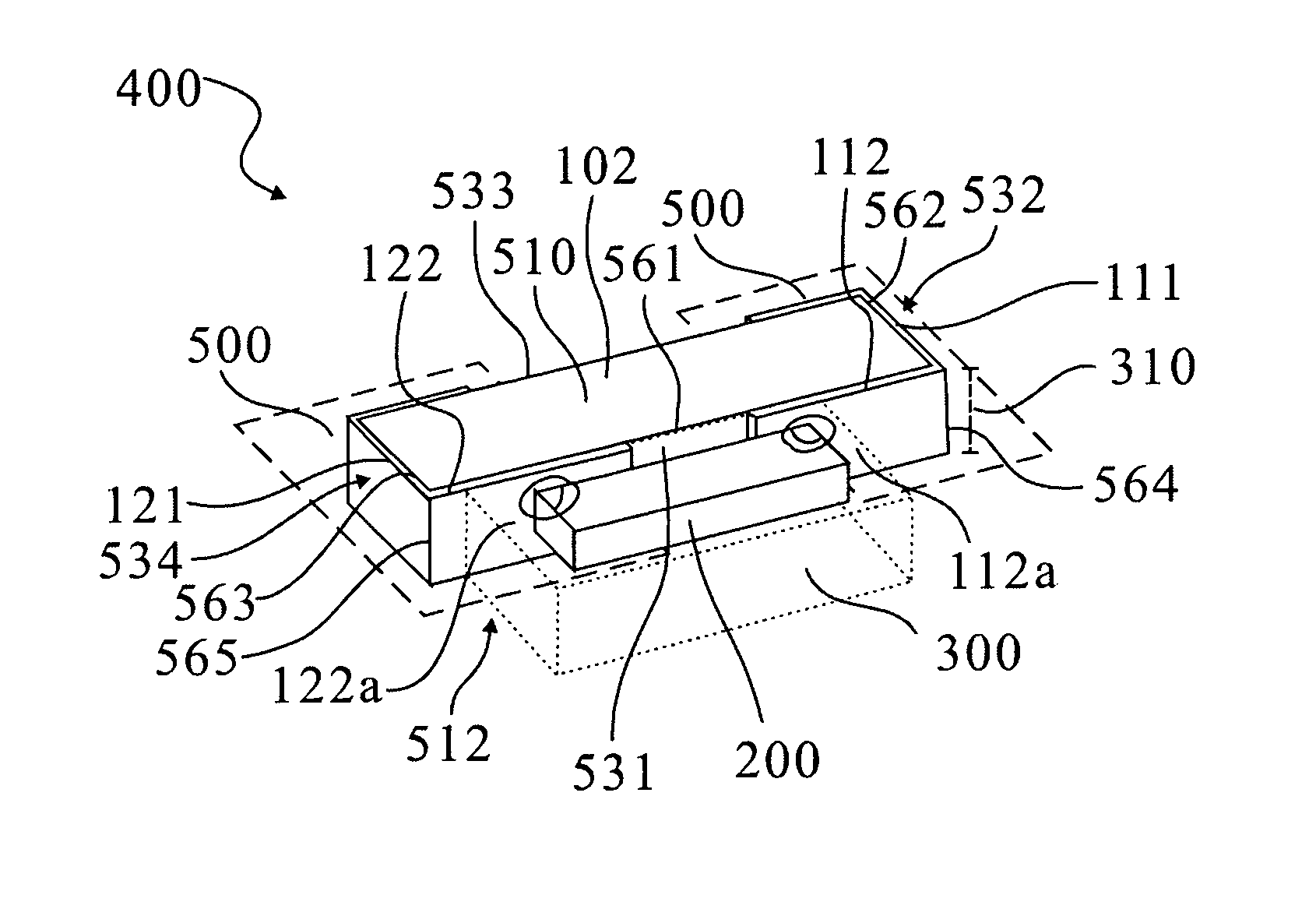
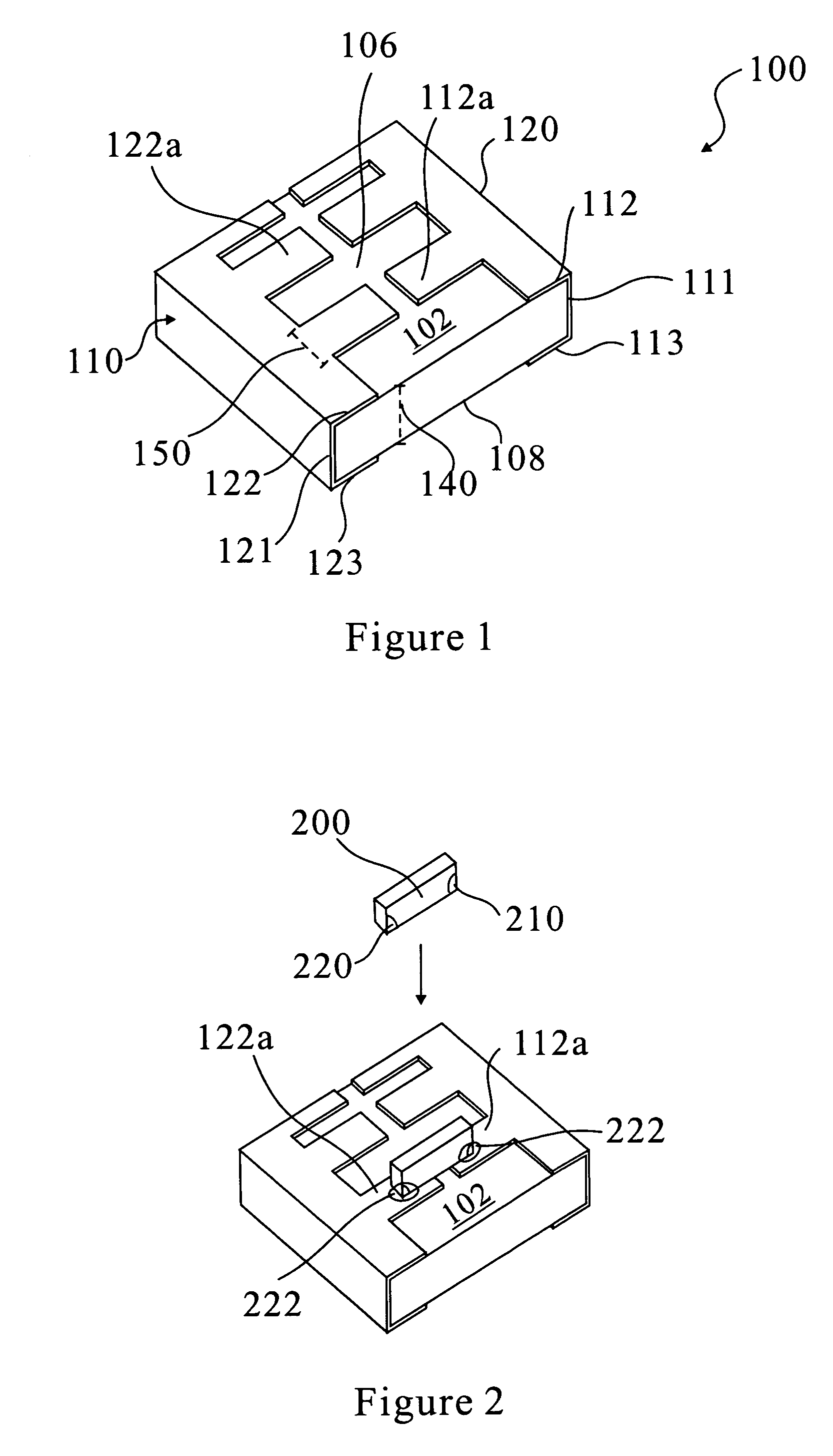
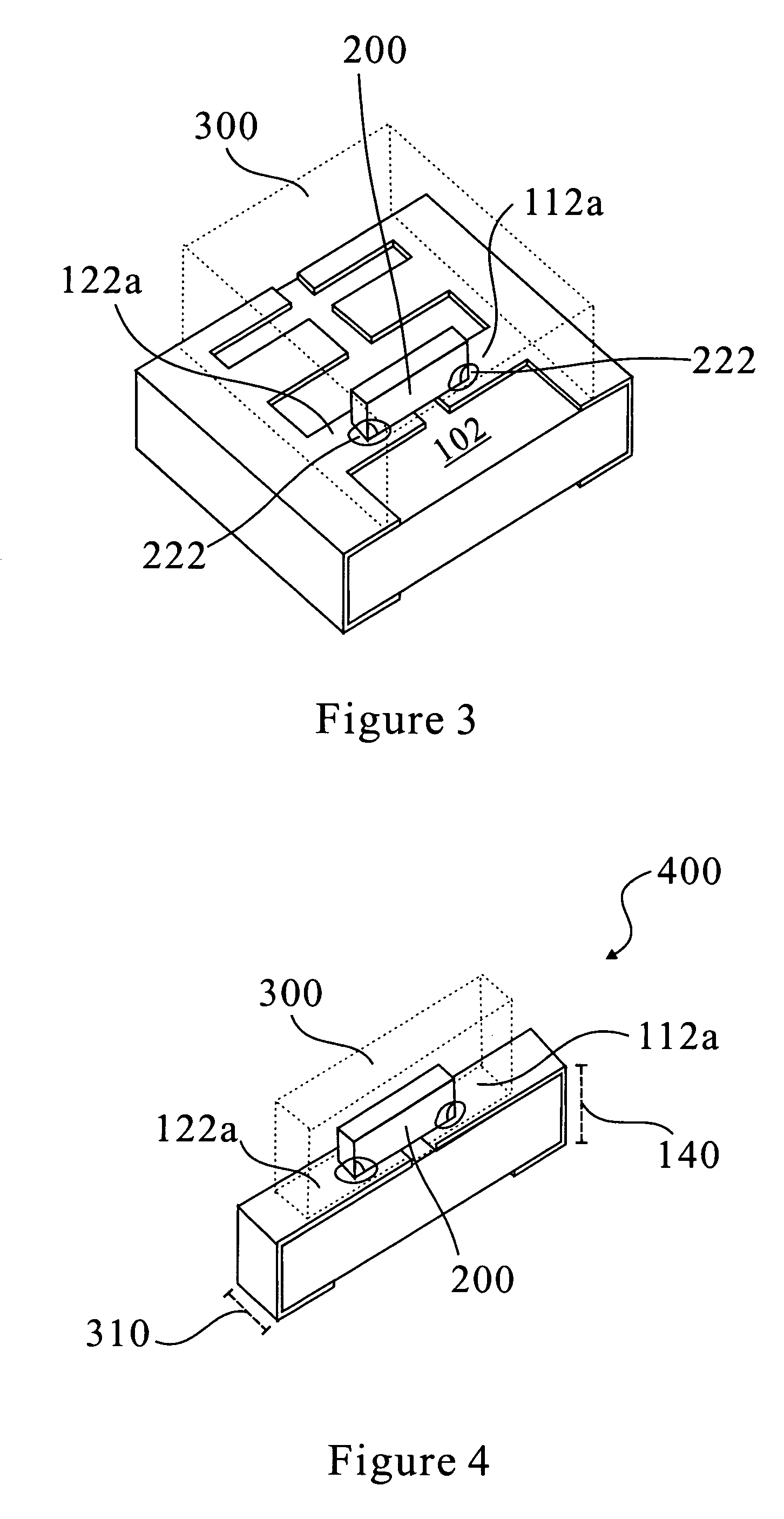
[0026]Refer to FIG. 1 and FIG. 2. FIG. 1 is a perspective view of a base apparatus in accordance with the present invention, and FIG. 2 is an exploded perspective view of the base apparatus in FIG. 1 when mounting an illuminating device. A base apparatus 100 in accordance with the present invention of an LED comprises a base 102 and two finger devices 110,120 including a first finger device 110 and a second finger device 120. The base 102 has a first surface 106, a second surface 108 and two opposite sides. The first surface 106 is opposite to the second surface 108.

[0027]The finger devices 110,120 are respectively mounted at the sides of the base 102 and are made of conductive material. Each of the ...


PUM

PropertyMeasurementUnit
heightaaaaaaaaaa
heightaaaaaaaaaa
heightaaaaaaaaaa

Abstract

A base apparatus includes a base and two finger devices. The base has a first surface and two opposite sides. The finger devices are respectively mounted on the sides of the base, are made of conductive material, and each of the finger devices has multiple fingers. The fingers are extended on the first surface of the base, wherein the fingers of a first finger device are arranged respectively corresponding to the fingers of a second finger device whereby each pair of corresponding fingers supports an illuminating device. The base has a height, each of the fingers has a width and the width is smaller than the height. When the LED is mounted onto a substrate, the LED can be mounted on the substrate by its side so that an entire assembly height of the LED is reduced and is equal to the width of the LED.

Description

RELATED APPLICATIONS[0001]The present application is based on, and claims priority from, Taiwan Application Serial Number 95123219, filed Jun. 27, 2006, the disclosure of which is hereby incorporated by reference herein in its entirety.BACKGROUND[0002]1. Field of Invention[0003]The present invention relates to a light emitting diode (LED). More particularly, the present invention relates to a light emitting diode that can be mounted on a substrate by its side to provide an ultra-thin profile.[0004]2. Description of Related Art[0005]Portable electric devices such as personal digital assistants (PDAs) or cell phones are increasingly common and popular. The current trend for those portable devices is towards light, thin, short and small profile. Structure, operation and appearance are emphasized in the compact design of these portable devices so that they are convenient to carry and are competitive in the market. Therefore, components of those compact portable devices must have a small...

Claims


Application Information

Patent Timeline
Patent Type & Authority Patents(United States)
IPC IPC(8): H01L27/15H01L31/12H01L33/00B23K1/00B23K5/00H01L33/56
CPCH01L33/486H01L24/16H01L2924/12041H01L2924/00
Inventor CHANG, CHENG-YI
Owner EVERLIGHT ELECTRONICS
Why Eureka
Try Eureka