

Multilayer ceramic circuit board having protruding portion and method for manufacturing the same
a ceramic circuit board and ceramic technology, applied in the direction of printed circuit manufacturing, printed circuit stress/warp reduction, printed circuit aspects, etc., can solve problems such as disposal, and achieve the effect of increasing flatness
- Summary
- Abstract
- Description
- Claims
- Application Information
AI Technical Summary
Benefits of technology
Problems solved by technology
Method used
Image

Examples
Embodiment Construction
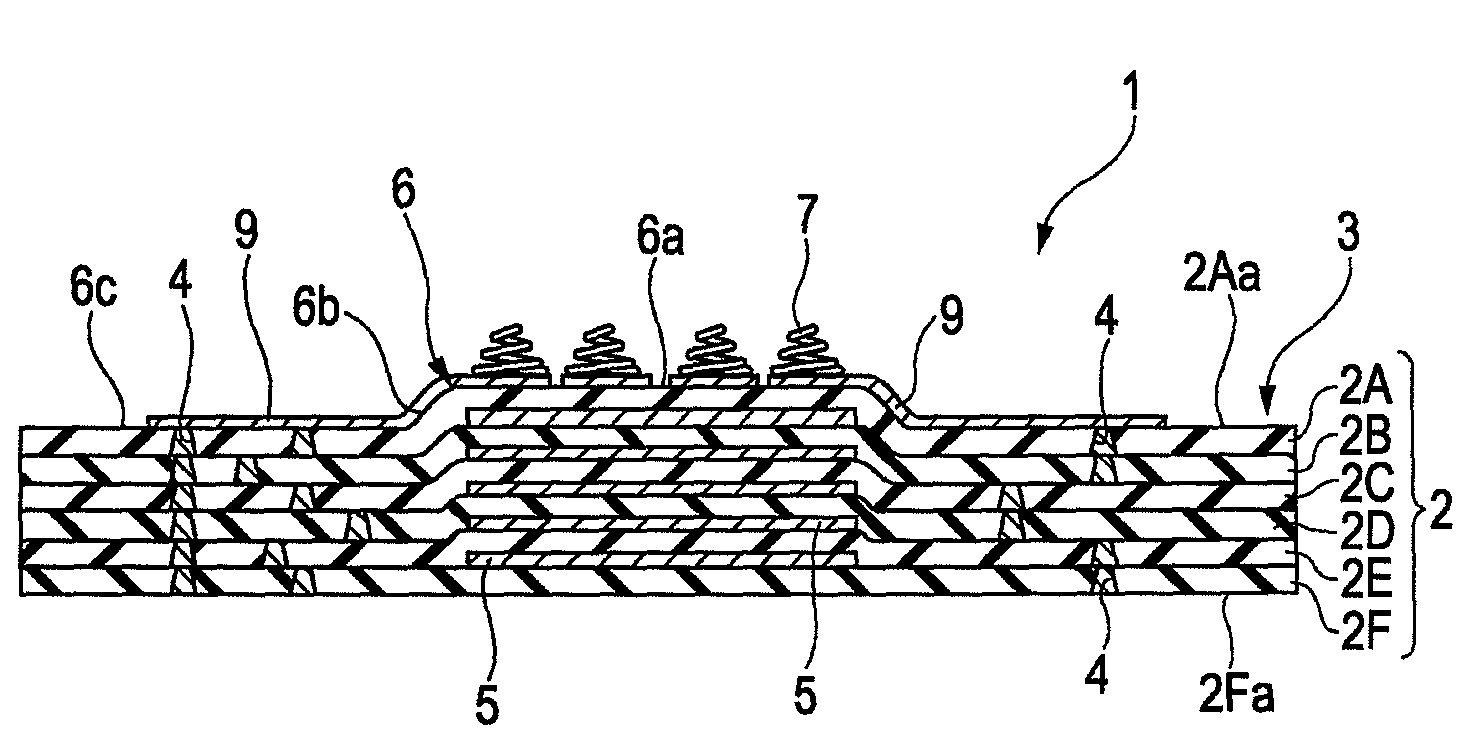
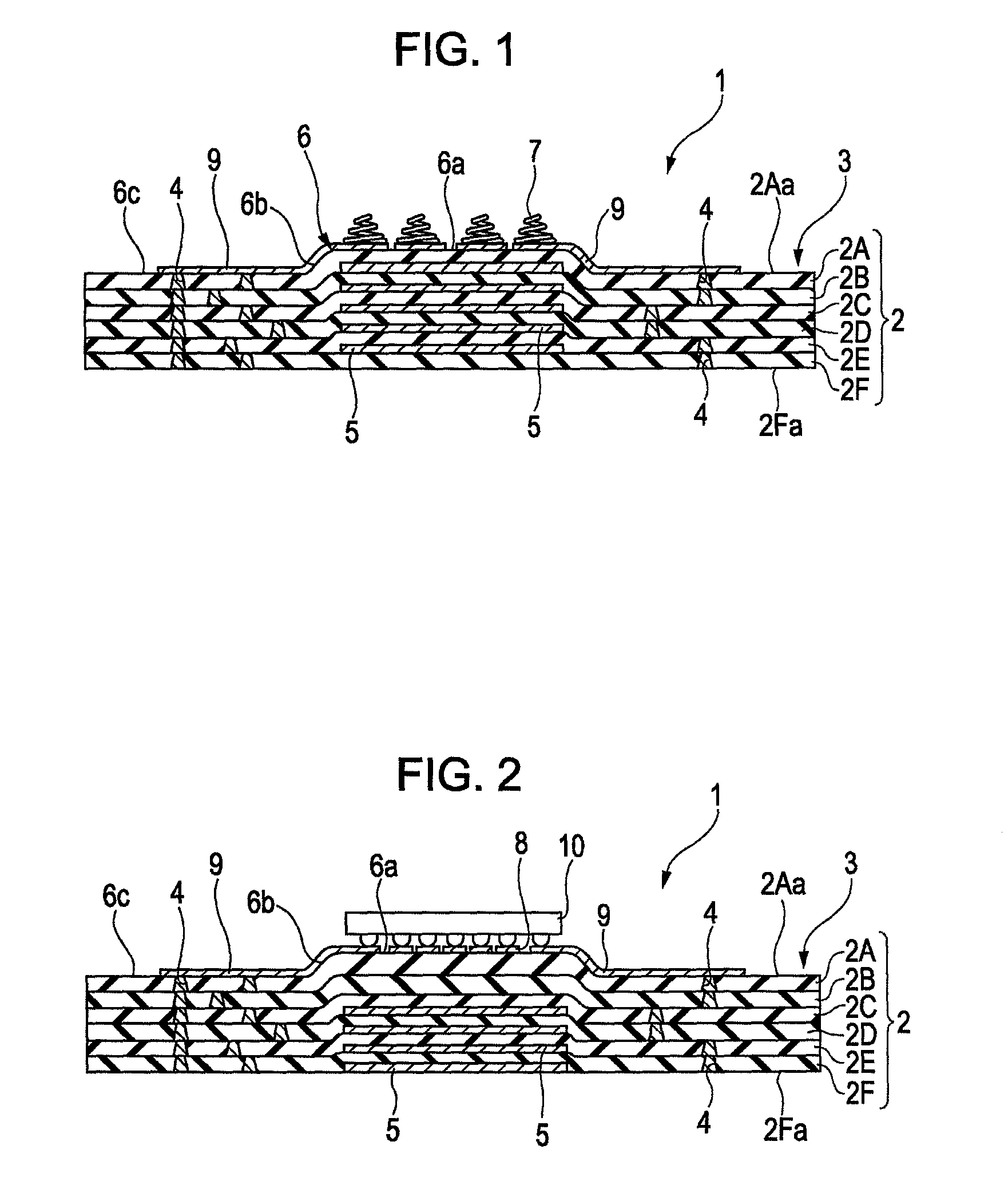
[0027]A multilayer ceramic circuit board and a method for manufacturing the multilayer ceramic circuit board according to an embodiment of the present invention will be described below with reference to the drawings.
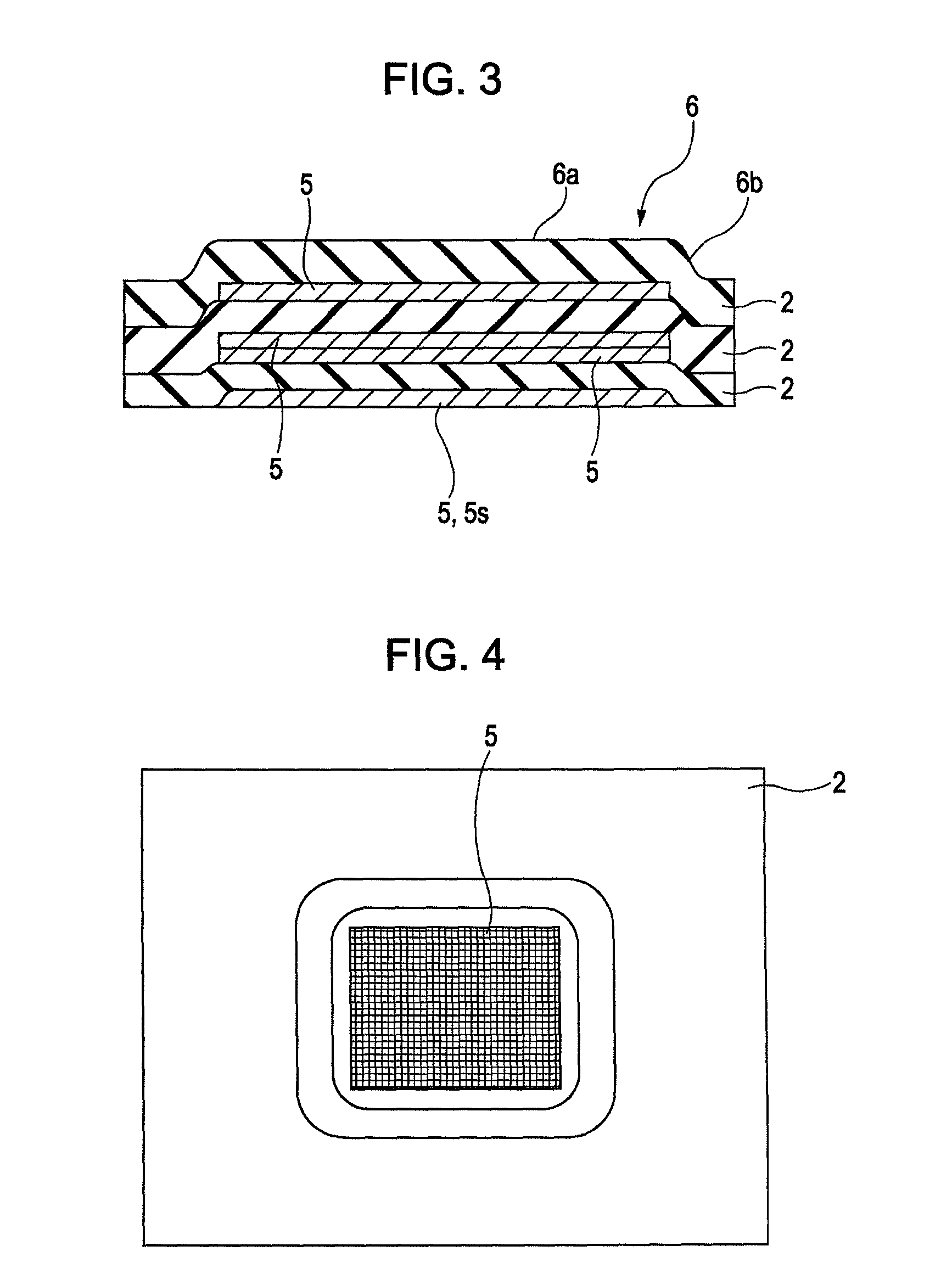
[0028]FIGS. 1 and 2 are each a longitudinal sectional view showing a multilayer ceramic circuit board 1 according to the embodiment. As shown in FIG. 1, the multilayer ceramic circuit board 1 includes a plurality of ceramic wiring layers 2 and lifting layers 5.
[0029]The plurality of ceramic wiring layers 2 are stacked vertically as shown in FIG. 1. In the multilayer ceramic circuit board 1 according to this embodiment, six ceramic wiring layers 2 are stacked. A top ceramic wiring layer 2A is designated as a first ceramic wiring layer 2A, and a bottom ceramic wiring layer 2F is designated as a sixth ceramic wiring layer 2F. The ceramic wiring layers are designated from the top to the bottom by a first ceramic wiring layer 2A, a second ceramic wiring layer 2B, . . . , a si...
PUM
| Property | Measurement | Unit |
|---|---|---|
| thickness | aaaaa | aaaaa |
| width | aaaaa | aaaaa |
| length | aaaaa | aaaaa |
Abstract
Description
Claims
Application Information