Unlock instant, AI-driven research and patent intelligence for your innovation.

Semiconductor device and semiconductor device manufacturing method

a semiconductor device and semiconductor technology, applied in semiconductor devices, capacitors, electrical devices, etc., can solve the problems of increasing contact resistance, reducing the amount of charge accumulated in the capacitor, and becoming difficult to employ sac etching in forming the contact hole of the capacitor, so as to reduce the contact resistance between the second conductive member and the contact plug, the effect of reducing the increase of current constriction and reducing the size of the semiconductor devi

Inactive Publication Date: 2011-08-30
PS4 LUXCO SARL
View PDF10 Cites 3 Cited by
  • Summary
  • Abstract
  • Description
  • Claims
  • Application Information

AI Technical Summary

Benefits of technology

"The present invention provides a semiconductor device and manufacturing method that can be miniaturized while maintaining adequate contact between a contact plug and a conductive member on the contact plug. This is achieved by using a contact plug with a small-diameter part and a large-diameter part, with the large-diameter part having a larger outer diameter than the small-diameter part and the connection face between the second conductive member and the large-diameter part. This reduces the outer diameter of the small-diameter part and allows for a smaller device size. The semiconductor device includes a first interlayer insulating film, a first conductive member, a bit-line interlayer insulating film, and a second interlayer insulating film. The manufacturing method includes forming a first resist mask and etching the first interlayer insulating film to form a first capacitor contact hole, removing the first resist mask, and etching the second interlayer insulating film to form a connection hole. The second conductive member is then formed to connect to the contact plug. The semiconductor device and manufacturing method provide a solution to the problem of miniaturization while maintaining adequate contact between the contact plug and the conductive member."

Problems solved by technology

This has led to a problematic decrease in the amount of charge accumulated in the capacitor.
However, as semiconductor devices become more miniaturized and thinner, it is becoming difficult to employ SAC etching in forming a capacitor contact hole.
However, even when using these conventional techniques, since the area of contact between the capacitor lower electrode and the capacitor contact plug is decreasing as semiconductor device become more miniaturized and thinner, the following problems arise.
One problem is that the contact resistance increases, due to the reduced area of contact between the capacitor lower electrode and the capacitor contact plug.
Another problem is that leak current increases, due to constriction of current at the connection section of the capacitor lower electrode and the capacitor contact plug.
The following problems also arise due to the reduced area of contact between the capacitor lower electrode and the capacitor contact plug.

Method used


Image

  • Semiconductor device and semiconductor device manufacturing method
  • Semiconductor device and semiconductor device manufacturing method
  • Semiconductor device and semiconductor device manufacturing method

Examples


Embodiment Construction

A semiconductor device and a manufacturing method thereof according to a first embodiment of the invention will be explained using FIGS. 1 to 7.

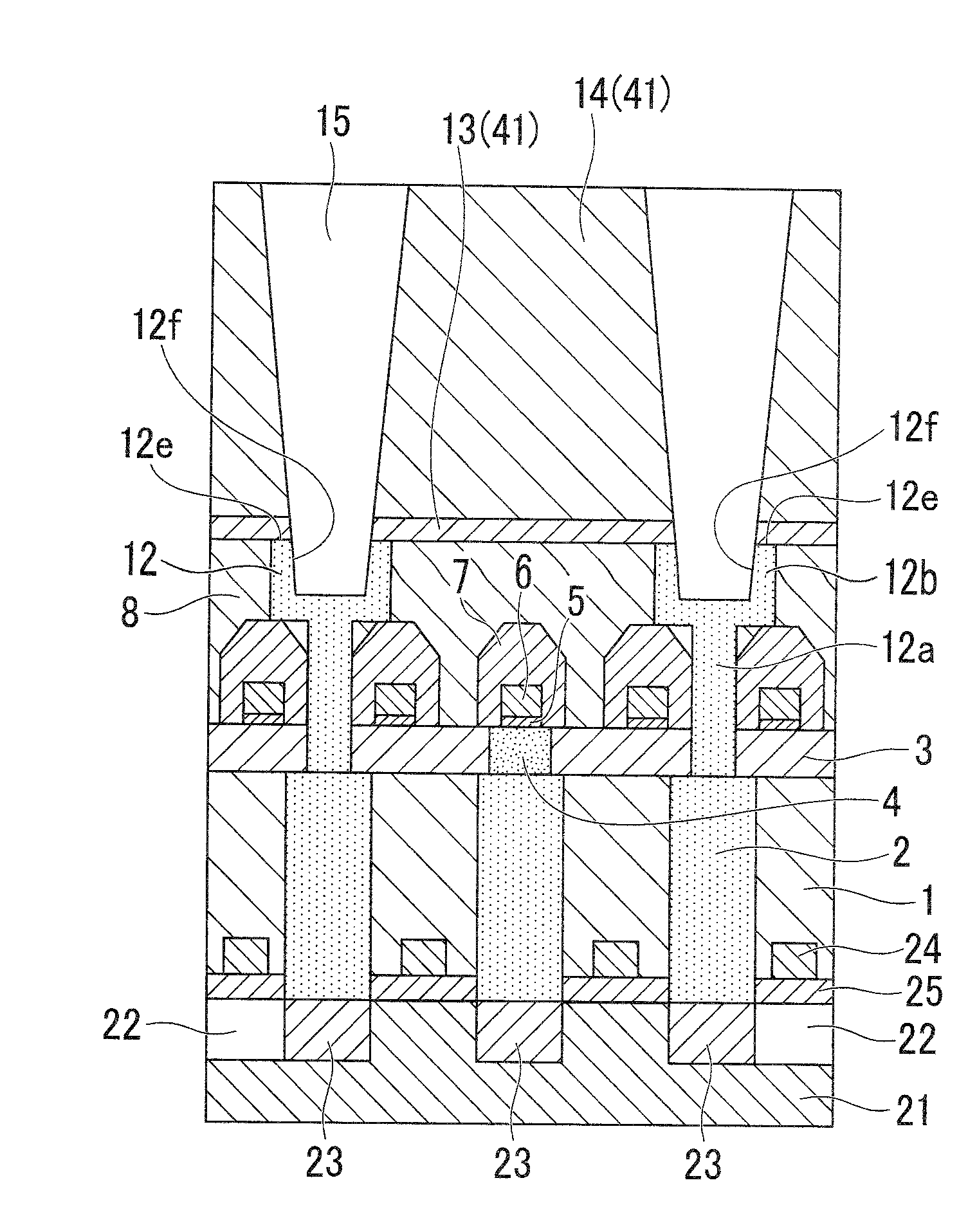
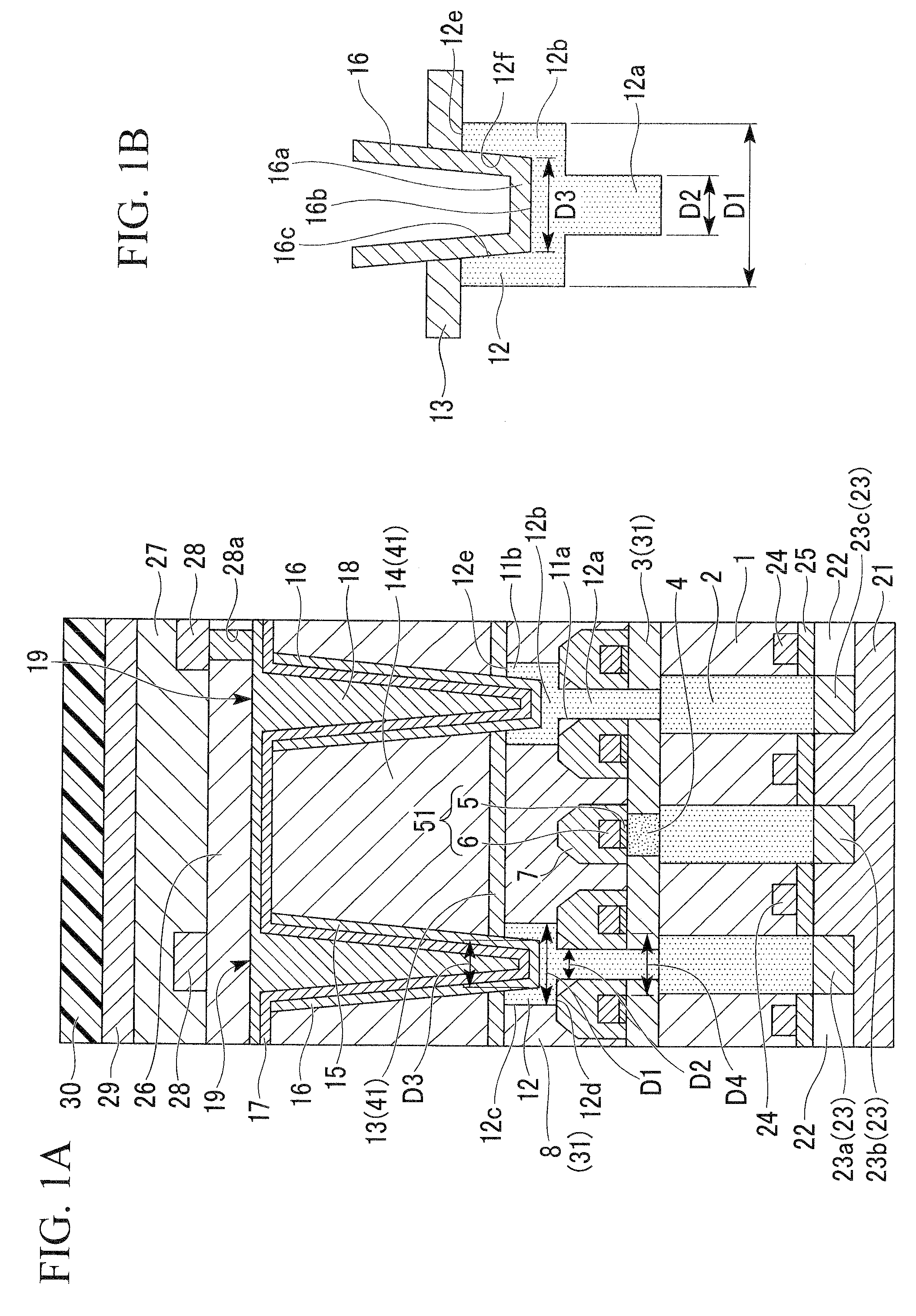
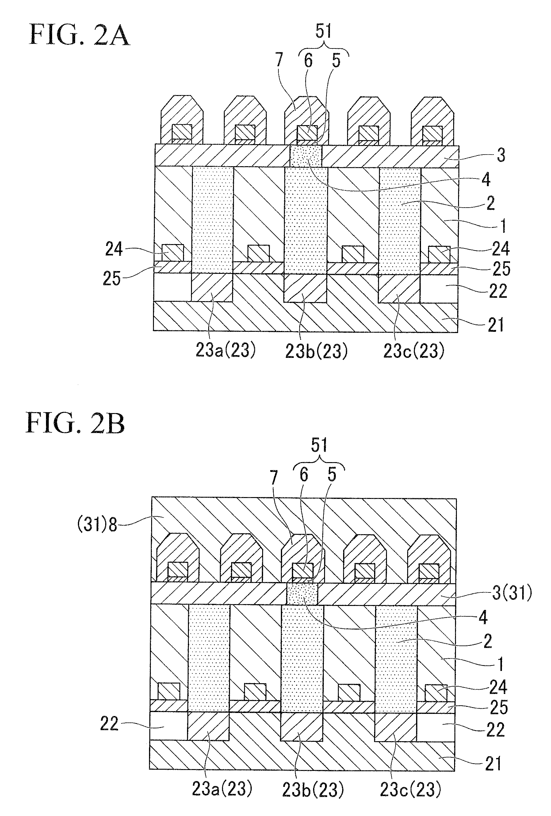
FIG. 1A is an explanatory view of a cross-sectional structure of a semiconductor device of the invention, and is a cross-sectional view in a direction parallel to a gate wiring. FIG. 1B is an enlarged view of one part of FIG. 1A. In the semiconductor device shown in FIGS. 1A and 1B, parts which are common to those of the semiconductor device of related art shown in FIG. 8 are designated by the same reference numerals, and are not repetitiously explained.

In FIG. 1A, a substrate 21 is such as a silicon substrate. An element isolation region (STI) 22 shown in FIG. 1A is formed on the substrate 21. A switching transistor is provided on the substrate 21. The switching transistor includes a gate electrode 24, a gate oxidization film 25, and an impurity dispersion layer 23 including sources 23a and 23c, and a drain 23b. A gate interlayer insulating...


PUM


Abstract

A semiconductor device includes: a first interlayer insulating film; a first conductive member provided lower than the first interlayer insulating film; a contact plug that penetrates through the first interlayer insulating film, and is electrically connected to the first conductive member, the contact plug including a small-diameter part, and a large-diameter part arranged on the small-diameter part, an outer diameter of the large-diameter part being larger than an outer diameter of the small-diameter part, and the outer diameter of the large-diameter part being larger than an outer diameter of a connection face between the second conductive member and the large-diameter part; and a second conductive member that is provided on the first interlayer insulating film, and is electrically connected to the contact plug.

Description

BACKGROUND OF THE INVENTION1. Field of the InventionThe present invention relates to a semiconductor device and a semiconductor device manufacturing method. The invention particularly relates to a semiconductor device and a semiconductor device manufacturing method that are suitable for application in a semiconductor device including a dynamic random access memory (DRAM) capacitor.Priority is claimed on Japanese Patent Application No. 2007-177188, filed Jul. 5, 2007, the content of which is incorporated herein by reference.2. Description of Related ArtMemory cells such as a DRAM include switching transistors and capacitors. With the advancement of minute work techniques, memory cells are becoming increasingly miniaturized. This has led to a problematic decrease in the amount of charge accumulated in the capacitor. To solve this problem, the height of the capacitor is increased by utilizing a capacitor over bit-line (COB) structure and forming a cup-shaped capacitor over the bit-line...

Claims


Application Information

Patent Timeline
Patent Type & Authority Patents(United States)
IPC IPC(8): H01L21/20
CPCH01L27/10855H01L28/40H01L27/10814H10B12/315H10B12/0335
Inventor NISHI, HIROO
Owner PS4 LUXCO SARL