Vertical gate-all-around TFET

a transistor and all-around technology, applied in the field of geometries of gate all-around transistor devices, can solve the problems of small leakage current that is highly sensitive to the applied voltage, conventional silicon device geometries and materials have experienced difficulty in maintaining switching speeds without incurring failures, and the dimension has shrunk below, so as to enhance the reliability of vertical tfet integrated circuits, the effect of low contact resistan

Active Publication Date: 2016-07-05
STMICROELECTRONICS INT NV
View PDF4 Cites 86 Cited by
  • Summary
  • Abstract
  • Description
  • Claims
  • Application Information

AI Technical Summary

Benefits of technology

[0008]A vertical TFET provides low-power, high-speed switching performance for transistors having critical dimensions below 7 nm. In one embodiment, the vertical TFET is implemented in silicon, using a gate-all-around (GAA) device architecture. The vertical GAA TFET is a linear, or 1-D, device in the form of a nanowire oriented transverse to planar front and back surfaces of the silicon substrate. The nanowire includes a lower drain region, a channel, and an upper source region, which are grown epitaxially from the doped well. The channel region is made of intrinsic silicon, while the source and drain regions are doped in-situ. An annular gate surrounds the channel region, capacitively controlling current flow through the channel from all sides. The source is electrically accessible via a front side contact, while the drain is accessed via a backside contact that provides low contact resistance and also serves as a heat sink.
[0009]Reliability of vertical TFET integrated circuits is enhanced by coupling the TFETs to electrostatic discharge (ESD) diodes. Both vertical and horizontal ESD diode configurations are described herein. ESD diodes provide protection for TFETs and other GAA transistors against high currents and voltages, especially in analog and I / O applications.

Problems solved by technology

As device dimensions have shrunk below 100 nm, however, conventional silicon device geometries and materials have experienced difficulty maintaining switching speeds without incurring failures such as, for example, leaking current from the device into the semiconductor substrate.
However, in reality, in the sub-threshold regime, there exists a small leakage current that is highly sensitive to the applied voltage.
Over time, the leakage current drains charge from the power supply, e.g., a mobile phone battery or a computer battery, thus necessitating more frequent recharging.

Method used


Image

  • Vertical gate-all-around TFET
  • Vertical gate-all-around TFET
  • Vertical gate-all-around TFET

Examples


second embodiment

[0041]FIG. 13 shows the vertical GAA TFET in which additional spacers are wrapped around the pillars between the gate structures 170 and the source and drain regions. A first spacer 185 is formed between the gate structures 170 and the source regions 154n,p, and a second spacer 185 is formed between the gate structures 170 and the drain regions 140, 142. The spacers 185, 186 can be made of SiN or SiC, for example.

third embodiment

[0042]FIG. 14 shows the vertical GAA TFET that features etched source contacts 190 in place of dual damascene contacts 182. The source contacts 190 differ from the dual damascene contacts 182 in that the source contacts 190 are formed by a subtractive etching process as opposed to forming and filling a trench, which is an additive process. Although either method can be used to form contacts to the source terminals of the GAA TFET, the front side source contacts 182 formed by the dual damascene process may offer lower contact resistance and a more flexible wire connection.

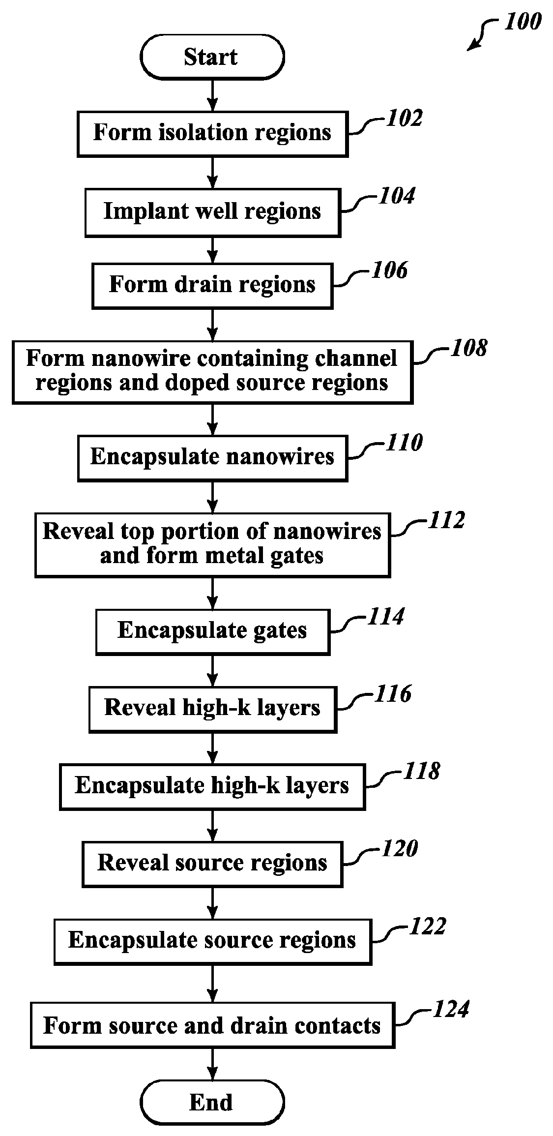
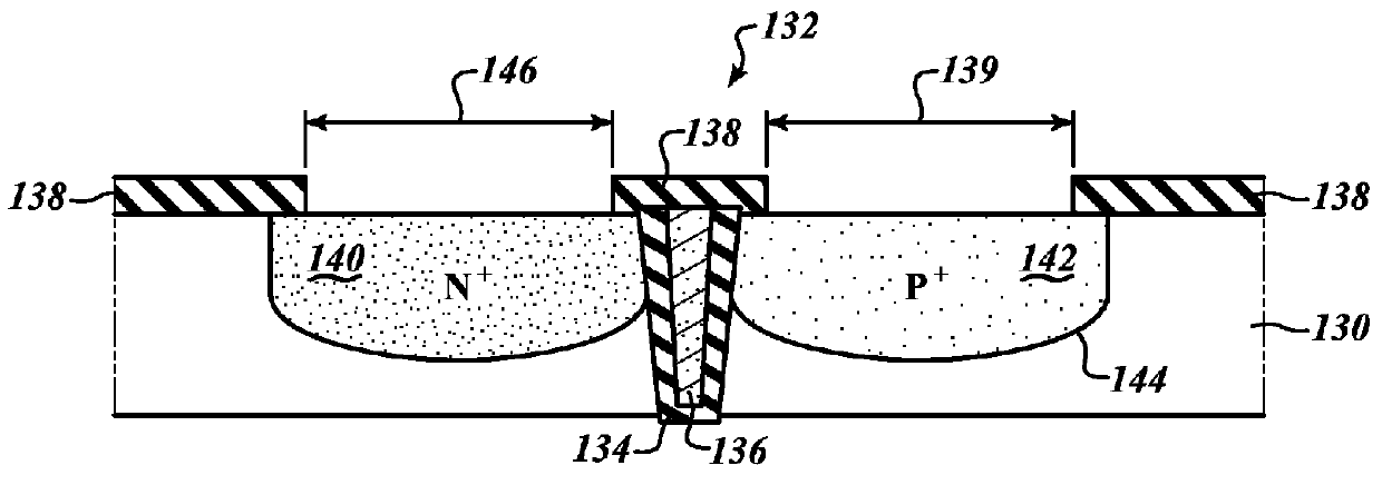
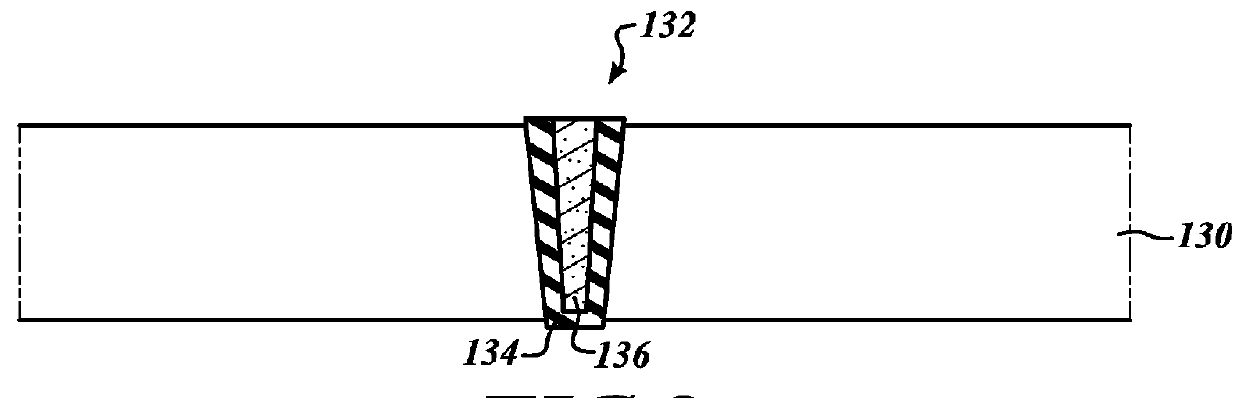
[0043]FIG. 15 shows steps in a method 200 of fabricating a vertical diode, according to one embodiment. The vertical diode can provide electrostatic discharge (ESD) protection for the vertical GAA TFET described above, to improve reliability. One advantage of the vertical diode is its small footprint, which is particularly useful in supporting GAA transistors used to form digital SRAM and DRAM arrays. The method 200...


PUM


Abstract

A vertical tunneling FET (TFET) provides low-power, high-speed switching performance for transistors having critical dimensions below 7 nm. The vertical TFET uses a gate-all-around (GAA) device architecture having a cylindrical structure that extends above the surface of a doped well formed in a silicon substrate. The cylindrical structure includes a lower drain region, a channel, and an upper source region, which are grown epitaxially from the doped well. The channel is made of intrinsic silicon, while the source and drain regions are doped in-situ. An annular gate surrounds the channel, capacitively controlling current flow through the channel from all sides. The source is electrically accessible via a front side contact, while the drain is accessed via a backside contact that provides low contact resistance and also serves as a heat sink. Reliability of vertical TFET integrated circuits is enhanced by coupling the vertical TFETs to electrostatic discharge (ESD) diodes.

Description

BACKGROUND[0001]1. Technical Field[0002]The present disclosure generally relates to various geometries for gate all-around transistor devices built on a silicon substrate and, in particular, to transistors that are suitable for low-power applications.[0003]2. Description of the Related Art[0004]Conventional integrated circuits incorporate planar field effect transistors (FETs) in which current flows through a semiconducting channel between a source and a drain, in response to a voltage applied to a control gate. The semiconductor industry strives to obey Moore's law, which holds that each successive generation of integrated circuit devices shrinks to half its size and operates twice as fast. As device dimensions have shrunk below 100 nm, however, conventional silicon device geometries and materials have experienced difficulty maintaining switching speeds without incurring failures such as, for example, leaking current from the device into the semiconductor substrate. Several new tec...

Claims


Application Information

Patent Timeline
Patent Type & Authority Patents(United States)
IPC IPC(8): H01L29/745H01L29/66H01L29/20H01L29/49H01L29/10H01L29/78H01L29/16H01L29/06H01L21/8238H01L21/00H01L21/28H01L27/148
CPCH01L29/0676H01L29/16H01L29/7827H01L29/1037H01L29/4966H01L29/495H01L29/20H01L29/66666H01L21/28008H01L29/1033B82Y10/00H01L29/66439H01L29/775H01L27/0814H01L27/092H01L29/7391H01L21/823807H01L21/823814H01L21/823828H01L21/823871H01L21/823878H01L21/823885H01L29/42392H10B12/056H10N70/826H01L21/823892H01L27/0928H01L29/0653H01L29/66977H01L29/78618H01L29/78642H01L29/78696H01L29/66795H01L29/66909H01L29/7855H01L29/7856H01L31/0392H01L33/04H01L2029/7858
Inventor ZHANG, JOHN H.
Owner STMICROELECTRONICS INT NV
Why Eureka
Try Eureka