
High power and high temperature semiconductor power devices protected by non-uniform ballasted sources

a technology of non-uniform ballasting and high-temperature semiconductors, applied in the direction of semiconductor devices, electrical appliances, transistors, etc., can solve the problems of device failure, high rdson resistance of devices provided for reliably operating at high power and high temperature, and the difficulty of conventional manufacturing and configuration of semiconductor power devices, so as to achieve the effect of reducing the rdson resistance and significant improvemen

Active Publication Date: 2011-08-30
ALPHA & OMEGA SEMICON LTD
View PDF5 Cites 0 Cited by
  • Summary
  • Abstract
  • Description
  • Claims
  • Application Information

AI Technical Summary

Benefits of technology

"The present invention provides a new and improved semiconductor power device with source ballasting to prevent thermal runaway and minimize the increase of resistance. The device has different transistor cells with varying ballasting resistances to effectively prevent the thermal runaway problem while minimizing the increase of resistance. The method of manufacturing the device includes selectively distributing the ballasting resistances based on the thermal dissipation and profile of the structure. The technical effects of the invention include reducing the significant Rdson increase and resolving the difficulties associated with uniform ballasting configurations."

Problems solved by technology

Conventional technologies of manufacturing and configuring semiconductor power devices are still confronted with a technical difficulty that devices provided for reliably operating at high power and high temperature usually have high Rdson resistance.
A temperature runaway condition may occur to cause a device failure.
The temperature runaway problem may occur to both the trench-gate DMOS devices as well as planar power MOSFET devices due to the underlined phenomenon of the negative temperature coefficient of the threshold voltage.
Significant increase of Rdson resistance often adversely affects the device performance due to a conventional configuration of uniformly implementing the source ballasting over the entire areas of the semiconductor power devices.
However, the Rdson is greatly increased and the device performance is adversely affected due the uniform addition of the source resistance by implementing the conventional ballasting technologies.

Method used


Image

  • High power and high temperature semiconductor power devices protected by non-uniform ballasted sources
  • High power and high temperature semiconductor power devices protected by non-uniform ballasted sources
  • High power and high temperature semiconductor power devices protected by non-uniform ballasted sources

Examples


Embodiment Construction

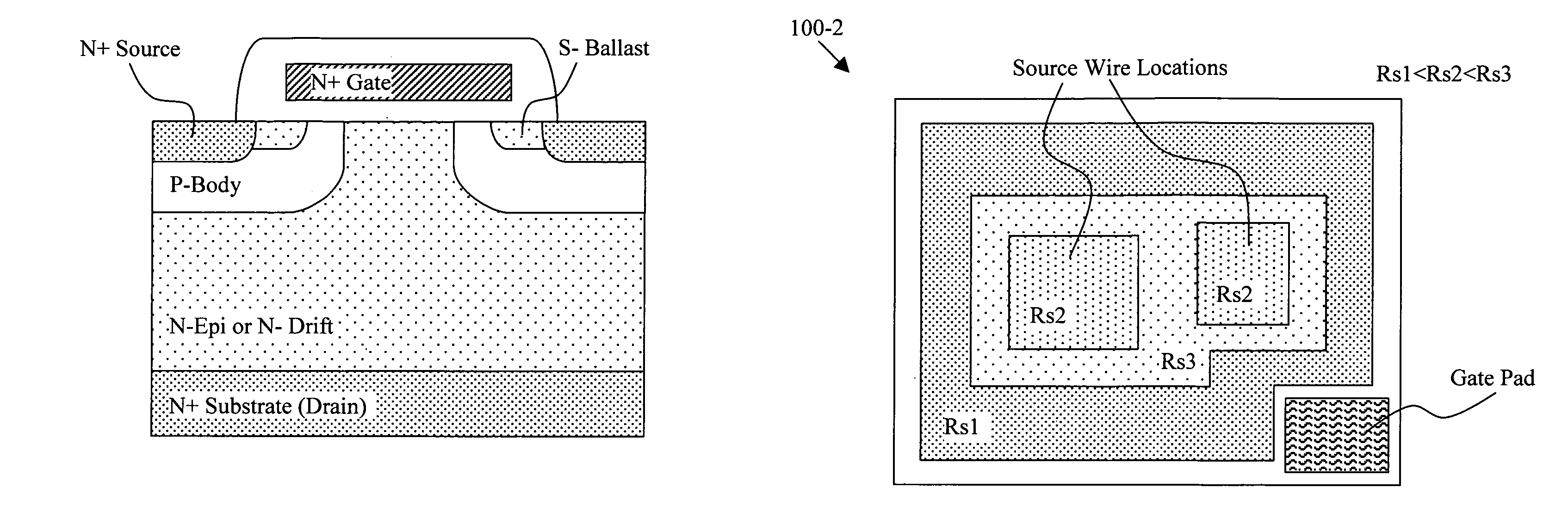
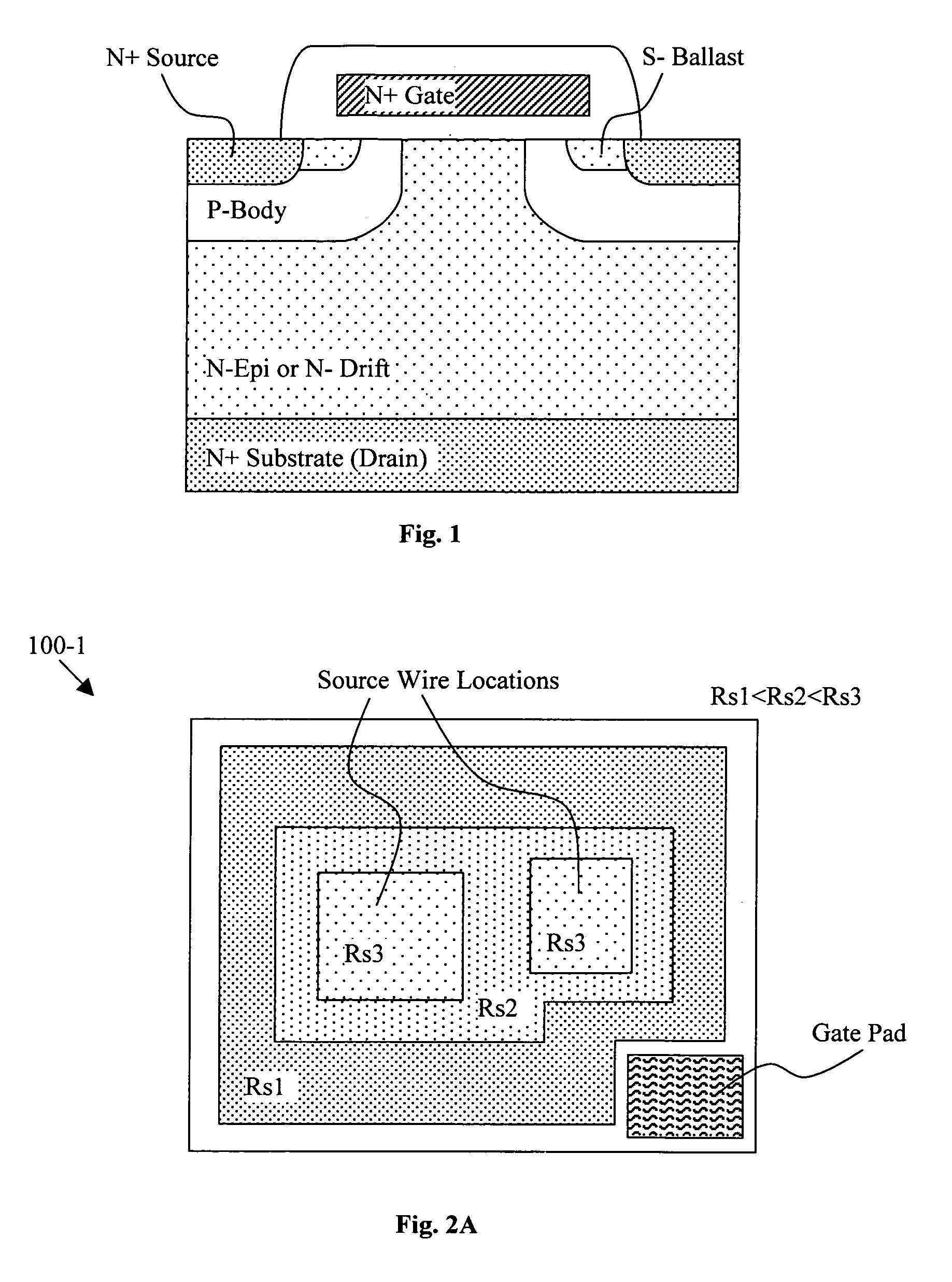
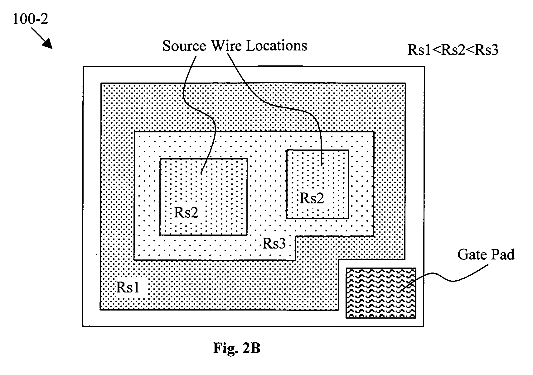
[0018]Referring to FIGS. 2A and 2B for two alternate top views of a semiconductor power device 100-1 and 100-2 respectively implemented with source ballasting configuration of this invention. In FIG. 2A, the entire surface of the device is divided into several areas include a gate bond pad area near the lower-left corner of the surface. The device further includes three different ballasting areas, i.e., Rs1, Rs2, and Rs3. The Rs3 area is an area designated as location for source wire bonding with area Rs2 surrounding the area Rs3 and a peripheral area Rs1 near the edges of the device surface. According to the actual inspection of device failures caused by thermal runaway problems, the damaged silicon usually occurs in five to fifteen seconds with a current of one to twenty amperes at a temperature of 180 to 200 degrees Celsius. The damages are observed mostly near or between the bond wires while the regions outside the wire bonding areas and under the bond wires rarely have any prob...


PUM


Abstract

This invention discloses a semiconductor power device disposed on a semiconductor substrate supporting an epitaxial layer as a drift region composed of an epitaxial layer. The semiconductor power device further includes a super-junction structure includes a plurality of doped sidewall columns disposed in a multiple of epitaxial layers. The epitaxial layer have a plurality of trenches opened and filled with the multiple epitaxial layer therein with the doped columns disposed along sidewalls of the trenches disposed in the multiple of epitaxial layers.

Description

BACKGROUND OF THE INVENTION[0001]1. Field of the Invention[0002]The invention relates generally to the vertical semiconductor power devices. More particularly, this invention relates to configurations and methods of manufacturing of vertical semiconductor power devices with transistor cells with non-uniform ballasted sources to protect the semiconductor power devices to reliably operate at high power and high temperature conditions.[0003]2. Description of the Prior Art[0004]Conventional technologies of manufacturing and configuring semiconductor power devices are still confronted with a technical difficulty that devices provided for reliably operating at high power and high temperature usually have high Rdson resistance. Specifically, high reliability is expected from power transistors designed for operating at high power, i.e., high voltage and current, and high temperature applications. One exemplary application is the power transistors implemented in the DC brushless motor contro...

Claims


Application Information

Patent Timeline
Patent Type & Authority Patents(United States)
IPC IPC(8): H01L29/66
CPCH01L29/0696H01L29/086H01L29/41741H01L29/41775H01L29/456H01L29/7802H01L24/05H01L29/7803H01L2924/13055H01L2924/13091H01L2924/1305H01L2924/1306H01L2224/0603H01L2924/00
Inventor HEBERT, FRANCOISBHALLA, ANUP
Owner ALPHA & OMEGA SEMICON LTD
Learn More