Robust semiconductor power devices with design to protect transistor cells with slower switching speed

a technology of semiconductor power devices and transistor cells, applied in electronic switching, relays, pulse techniques, etc., can solve the problems of device damage, relatively large current and voltage spikes, and transistor cells with slower switching speed in power devices are often vulnerable to over-current damage, so as to improve device configuration and reduce significant rdson increase , the effect of slowing down

Active Publication Date: 2009-09-03
ALPHA & OMEGA SEMICON LTD
View PDF17 Cites 11 Cited by
  • Summary
  • Abstract
  • Description
  • Claims
  • Application Information

AI Technical Summary

Benefits of technology

[0010]It is therefore an aspect of the present invention to provide a new and improved device configuration and method of manufacturing the semiconductor power device with specially arranged faster and slower switching transistor cells and providing additional source ballasting to the slower switching transistor cells for protecting these cells during the operations of turning off transitions. The slower transistor cells are designed to remain on longer while other transistor cells are turned off during a turning off operation. Instead of using a uniform ballasting configuration, only the slower switching transistor cells are added with ballasting protection such that the significant Rdson increase may be reduced and the above-discussed difficulties can be resolved. By designing a sufficient number of the transistors cells to be slower switching, the turn-off power will be safely spread among those cells, and not just focused on very few cells. Ballast resistors ensure even current distribution among the slow transistor cells therefore increasing the robustness.
[0011]Specifically, it is an aspect of the present invention to provide a new and improved device configuration and method of manufacturing the semiconductor power device by varying the amount of ballasting to strengthen the slower switching transistor cells with increased robustness to handle the power of high power and high voltage in the switching off transitions. Since only the slower transistor cells are adjusted, the overall increase of the Rdson in this invention is reduced and the additional area required for ballasting the transistor cells is also reduced. Specifically, the semiconductor power device is designed to have faster switching transistor cells and slower switching transistor cells. Only the slower switching transistor cells are designed and manufactured to have ballasting resistors to increase the robustness. The slower switching transistor cells can also be optimized for the high turn-off load by adjusting properties such as the cell density, ballast resistor values, and the percentage of slower switching transistor cells. Effective protection of the device against damages caused by the transitions of voltage and current during the turning off operations can therefore be achieved. The source ballasting distributions are selectively designed and manufactured in the semiconductor power devices with effective protection while minimizing the increase of the resistance and required silicon areas.
[0012]Briefly in a preferred embodiment this i

Problems solved by technology

Conventional technologies of manufacturing and configuring semiconductor power devices are still confronted with a technical difficulty that the transistor cells with slower switching speed in the power devices are often vulnerable to over-current damages when the power devices are implemented for switching off an electric connection.
In this initial transient state, the switch on or off operations causes a relatively large current and voltage spike.
The voltage and current spikes may cause sparks and EMI in the electronic device and may lead to device damages and poor reliability.
However this leads to problems that will be explained later.
Unfortunately, in the slow turning on or turning off operations, both high current and high voltage appears across the drain and source during the transition period, which can cause problems under certain conditions shown in FIG. 1B.
During a switching off operation, the slower transistor

Method used


Image

  • Robust semiconductor power devices with design to protect transistor cells with slower switching speed
  • Robust semiconductor power devices with design to protect transistor cells with slower switching speed
  • Robust semiconductor power devices with design to protect transistor cells with slower switching speed

Examples


Embodiment Construction

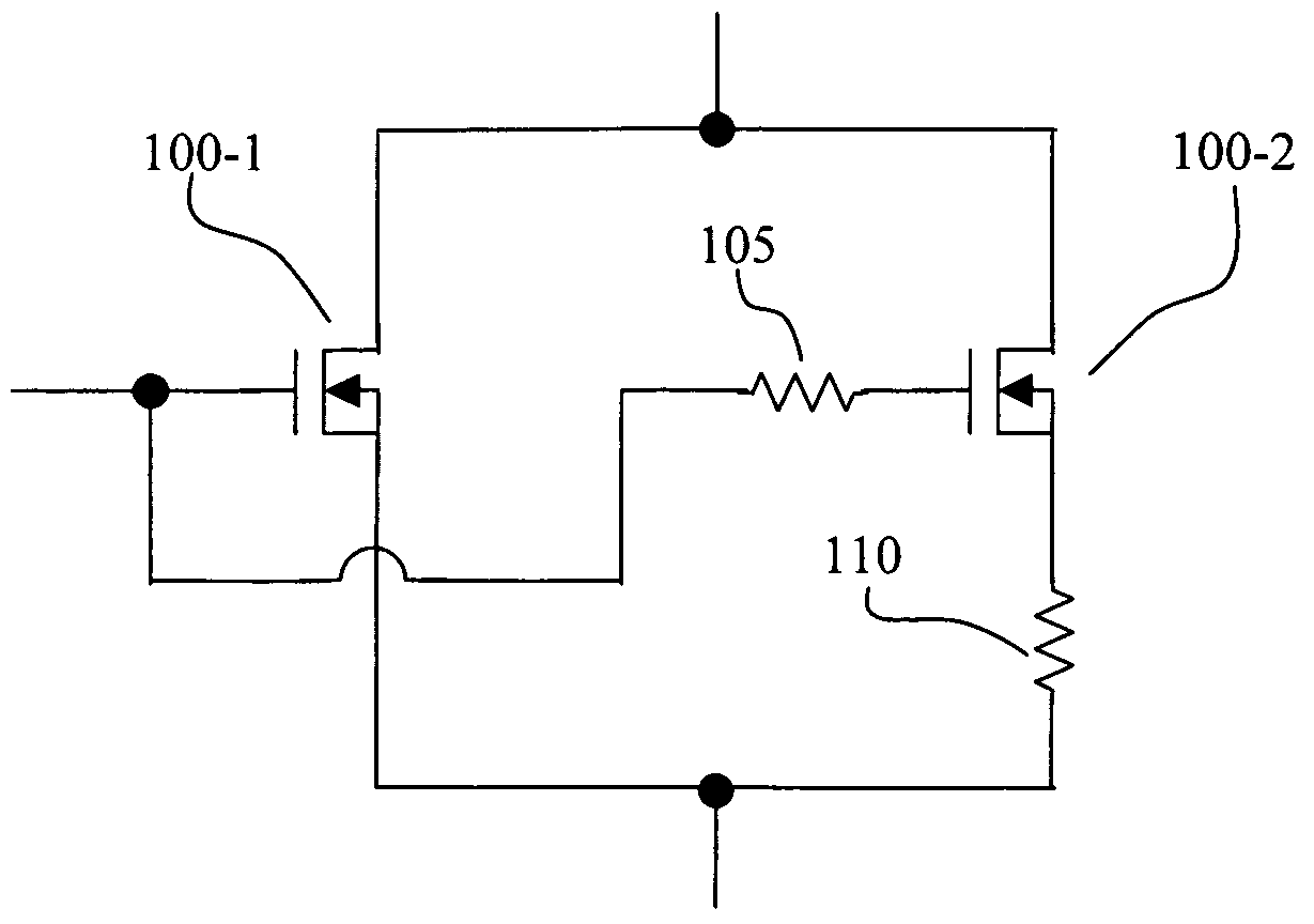
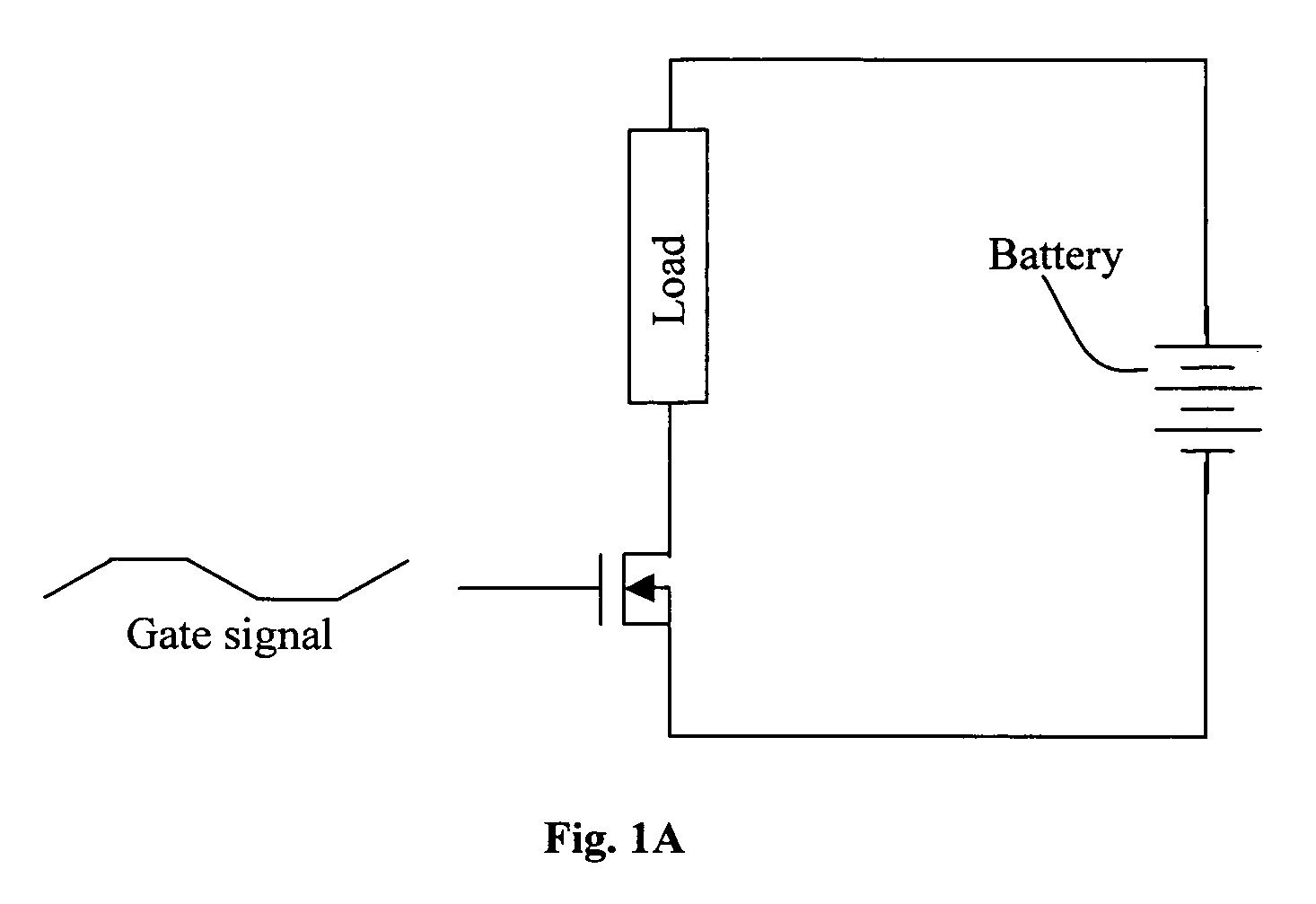
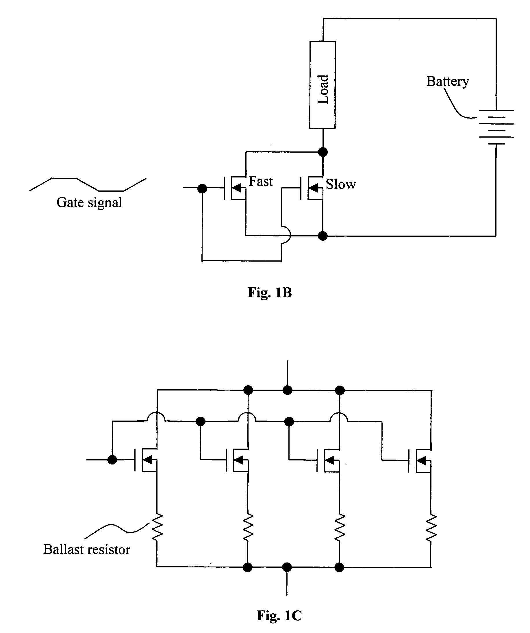
[0019]Referring to FIG. 2 for a circuit diagram for illustrating the improved circuit configuration to resolve the difficulties encountered in the convention semiconductor power devices implemented to switch on and off an electronic device. The semiconductor power device includes a first MOSFET 100-1 and a second MOSFET 100-2 connected in parallel and each receives a gate signal to function as a switch. The first MOSFET 100-1 is a fast switch and a second MOSFET 100-2 as a slow switch. In order to protect the slower switching MOSFET 100-2, a ballasting resistor 110 is added to the second MOSFET 100-2. When a gate signal is received to turn off the electric current, the first MOSFET 100-1 is turned off first while the second MOSFET 100-2 is a slower switching MOSFET and still remains at an on state. In this embodiment, a gate resistor 105 is added to the second MOSFET 100-2. The gate resistor 105 along with the natural capacitance of the gate, form a resistor-capacitor (RC) circuit. ...


PUM

PropertyMeasurementUnit
Lengthaaaaaaaaaa
Concentrationaaaaaaaaaa
Electrical resistanceaaaaaaaaaa

Abstract

This invention discloses a power switch that includes a fast-switch semiconductor power device and a slow-switch semiconductor power device controllable to turn on and off a current transmitting therethrough. The slow-switch semiconductor power device further includes a ballasting resistor for increasing a device robustness of the slow switch semiconductor power device. In an exemplary embodiment, the fast-switch semiconductor power device includes a fast switch metal oxide semiconductor field effect transistor (MOSFET) and the slow-switch semiconductor power device includes a slow switch MOSFET wherein the slow switch MOSFET further includes a source ballasting resistor.

Description

BACKGROUND OF THE INVENTION[0001]1. Field of the Invention[0002]The invention relates generally to the semiconductor power devices. More particularly, this invention relates to configurations and methods of manufacturing of semiconductor power devices comprise transistor cells with non-uniform cell characteristics of robustness to protect the slow switching power semiconductor devices for improving the device reliability.[0003]2. Description of the Prior Art[0004]Conventional technologies of manufacturing and configuring semiconductor power devices are still confronted with a technical difficulty that the transistor cells with slower switching speed in the power devices are often vulnerable to over-current damages when the power devices are implemented for switching off an electric connection. Specifically, when an electrical connection is switched on or off and before the operation reaches a steady state, a transient state takes place. In this initial transient state, the switch on...

Claims


Application Information

Patent Timeline
IPC IPC(8): H01H47/00H01H11/00
CPCH01L29/0696H01L29/0856H01L29/086H01L29/7803Y10T29/49105H03K17/164H01L2924/0002H01L29/7813H01L2924/00H03K17/04123H03K17/08122H03K17/122H01H49/00H03K17/687
Inventor LUI, SIK K.BHALLA, ANUP
Owner ALPHA & OMEGA SEMICON LTD
Why Eureka
Try Eureka