Gettering contaminants for integrated circuits formed on a silicon-on-insulator structure

Inactive Publication Date: 2011-09-13
MICRON TECH INC +1
View PDF43 Cites 4 Cited by
  • Summary
  • Abstract
  • Description
  • Claims
  • Application Information

AI Technical Summary

Benefits of technology

[0009]Yet another aspect is an integrated circuit formed on a semiconductor-on-insulator structure configured to attract contaminants. Contaminant attractor regions are formed using ion implantation into a semiconductor layer of the semiconductor-on-insulator structure. The semiconductor layer is located above a buried oxide layer of the semiconductor-on-insulator structure. An active region of the semiconductor layer of the semiconductor-on-insulator structure includes a dummy stripe and an active stripe. The dummy stripe is disposed at or proximate to an outer border of the active region. The ion implantation is into the dummy stripe for formation of the contaminant attractor regions therein. The contaminant attractor regions are for gettering at least a portion of the contaminants in the active region to the first contaminant attractor regions. At least one dielectric layer is disposed on the upper surface of the buried oxide layer including extending laterally along sides of the dummy stripe. The at least one dielectric layer at least inhibits lateral migration of the contaminants from the contaminant attractor regions of the dummy stripe to the active stripe when the semiconductor-on-insulator structure is exposed to a thermal cycle sufficient to mobilize the contaminants.
[0010]Still yet another aspect is a method of forming a semiconductor-on-insulator structure configured to attr

Problems solved by technology

However, DRAM conventionally has relatively slow access time.
Contaminants remain a problem in forming integrated circuits.
This problem is exacerbated in silicon-on-insulator

Method used


Image

  • Gettering contaminants for integrated circuits formed on a silicon-on-insulator structure
  • Gettering contaminants for integrated circuits formed on a silicon-on-insulator structure
  • Gettering contaminants for integrated circuits formed on a silicon-on-insulator structure

Examples


Example

DETAILED DESCRIPTION OF THE DRAWINGS

[0028]In the following description, numerous specific details are set forth to provide a more thorough description of the specific embodiments of the invention. It should be apparent, however, to one skilled in the art, that the invention may be practiced without all the specific details given below. In other instances, well-known features have not been described in detail so as not to obscure the invention. For ease of illustration, the same number labels are used in different diagrams to refer to the same items, however, in alternative embodiments the items may be different.

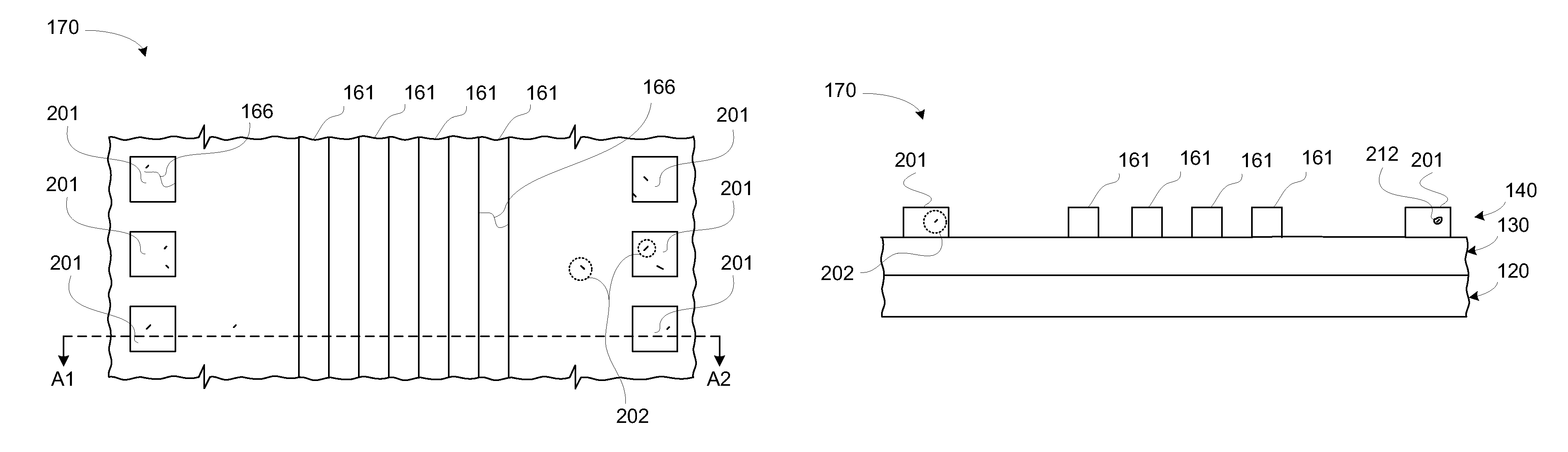
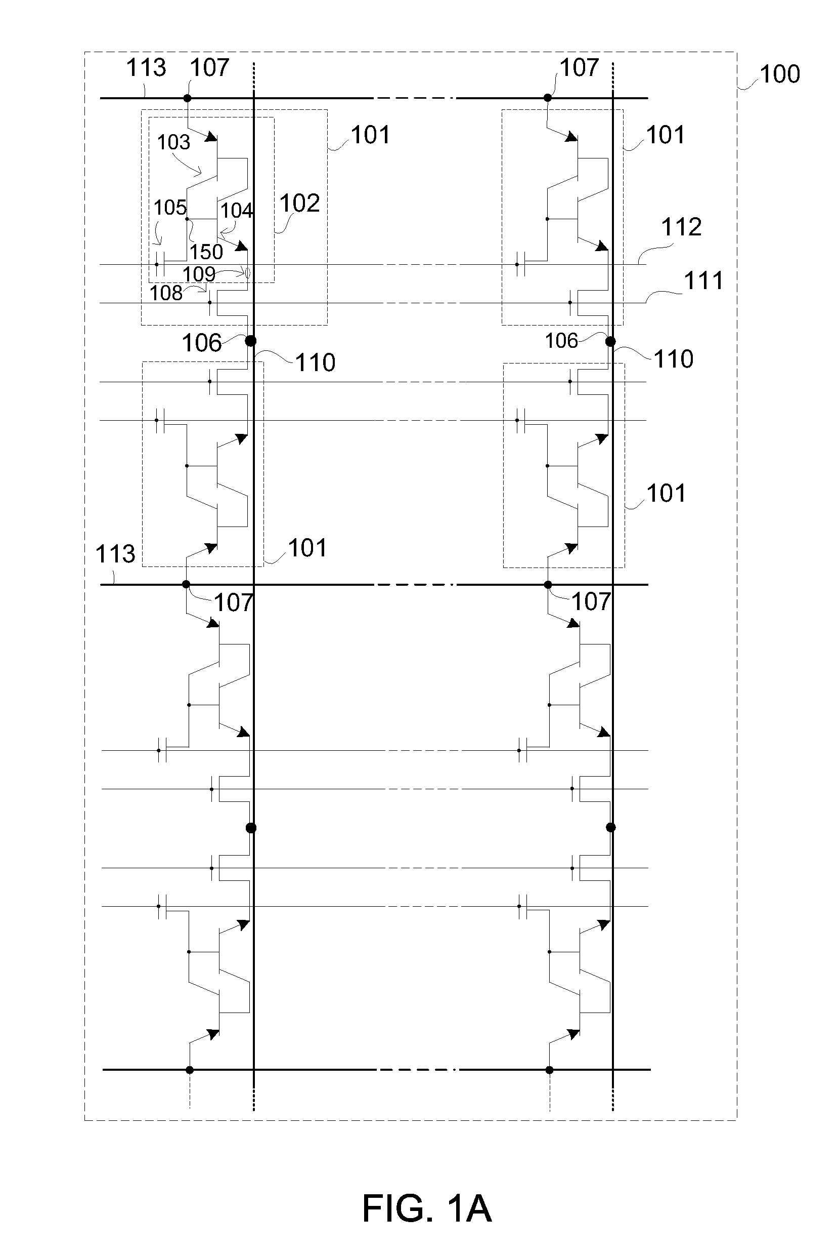
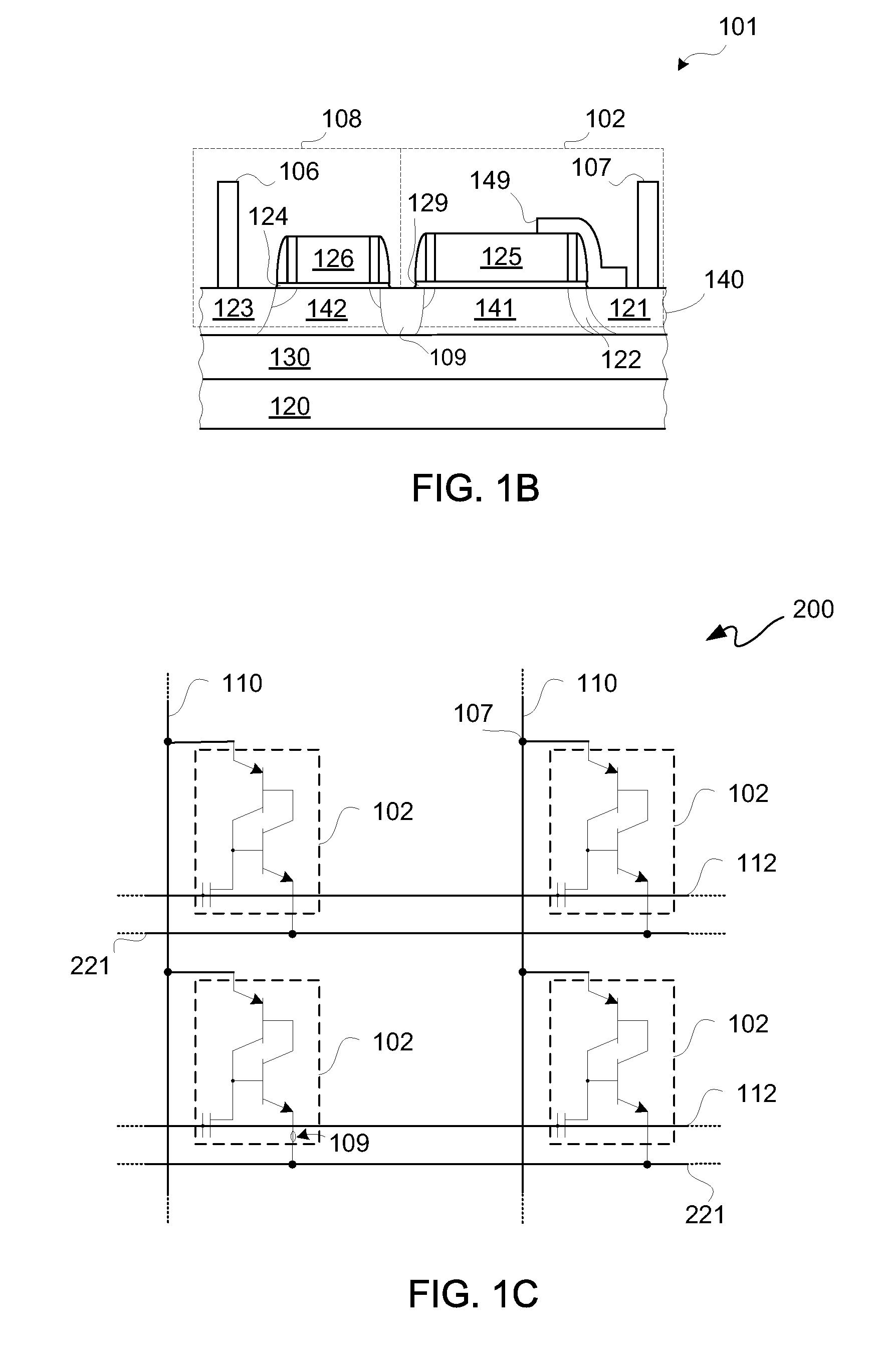
[0029]FIG. 1A is a schematic diagram depicting an exemplary embodiment of a memory array 100. Memory array 100 includes thyristor-based memory devices 101. Pairs of memory devices 101 may be commonly coupled at a bitline contact 106 for connection to a bitline 110 and may be commonly coupled at a supply voltage contact 107 for connection to a supply voltage line 113. Voltage ...


PUM


Abstract

Gettering contaminants for formation of integrated circuits on a semiconductor-on-insulator structure is described. A semiconductor-on-insulator structure is configured to attract contaminants. Contaminant attractor regions are formed using ion implantation into a semiconductor layer of the semiconductor-on-insulator structure. The semiconductor layer is located above a buried insulator layer of the semiconductor-on-insulator structure. The contaminant attractor regions are spaced away from active regions. Tiles are located on an upper surface of the buried insulator layer. The contaminant attractor regions are formed adjacent to, in close proximity to, or in the tiles. At least one dielectric layer laterally adjacent to the tiles and is disposed on the upper surface of the buried insulator layer. The at least one dielectric layer at least inhibits lateral migration of contaminants to the active regions.

Description

FIELD[0001]One or more aspects of the invention generally relate to integrated circuits and, more particularly, to gettering contaminants for formation of integrated circuits on a semiconductor-on-insulator structure, for example a silicon-on-insulator structure.BACKGROUND[0002]Conventionally, semiconductor memories, such as static random access memory (“SRAM”) and dynamic random access memory (“DRAM”), are in widespread use. DRAM is very common due to its high density with a cell size typically between 6F2 and 8F2, where F is a minimum feature size. However, DRAM conventionally has relatively slow access time. SRAM access time is conventionally an order of magnitude faster than DRAM. Though, an SRAM cell is commonly made of four transistors and two resistors or of six transistors, thus leading to a density of approximately 60F2 to 100F2.[0003]Memory designs based on a negative differential resistance (“NDR”) cell, such as a thyristor cell, have been introduced as a replacement for ...

Claims


Application Information

Patent Timeline
IPC IPC(8): H01L21/84
CPCH01L21/3226H01L21/84H01L27/1027H01L27/1203
Inventor BANNA, SRINIVASA R.ROBINS, SCOTT
Owner MICRON TECH INC
Why Eureka
Try Eureka