Adaptive bias circuit and system thereof

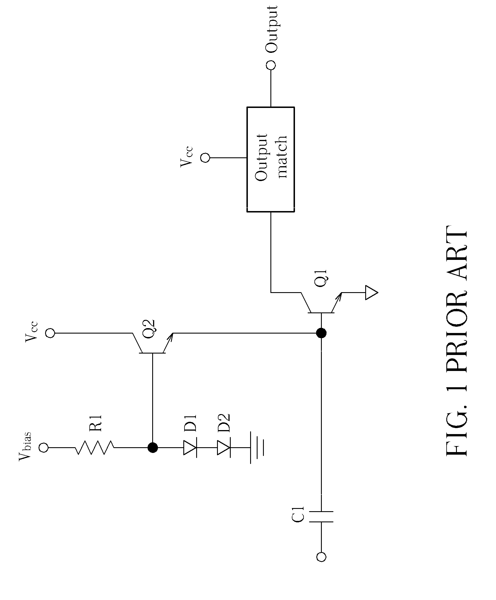
a bias transistor and bias transistor technology, applied in the direction of rf amplifiers, amplifiers with semiconductor devices/discharge tubes, gain control, etc., can solve the problems of inability to provide an agile adaptive current response with changes in input power, and the adaptive bias current provided by the bias transistor emitter qb>2/b> may not be large enough to keep the amplifier operating in the linear region

Active Publication Date: 2011-09-27
RICHWAVE TECH CORP
View PDF1 Cites 10 Cited by
  • Summary
  • Abstract
  • Description
  • Claims
  • Application Information

AI Technical Summary

Problems solved by technology

In some cases, as the input power increases, the adaptive bias current provided by the emitter of the bias transistor Q2 may not be large enough to keep the amplifier operating in the linear region.
This architecture emits more adaptive bias current with increased input power through the bias transistor 412, but is not able to provide an agile adaptive current response with changes in the input power.

Method used


Image

  • Adaptive bias circuit and system thereof
  • Adaptive bias circuit and system thereof
  • Adaptive bias circuit and system thereof

Examples


Embodiment Construction

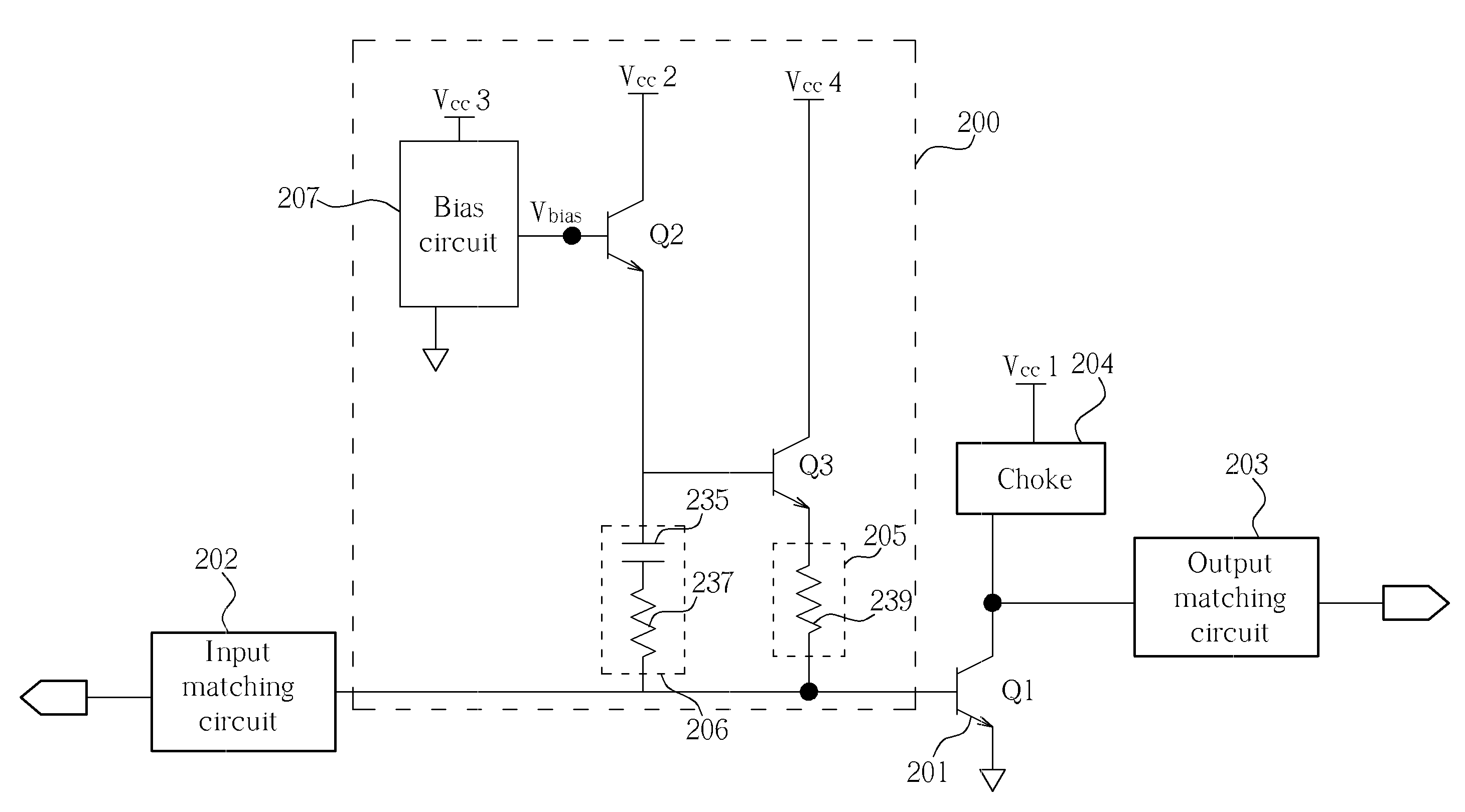
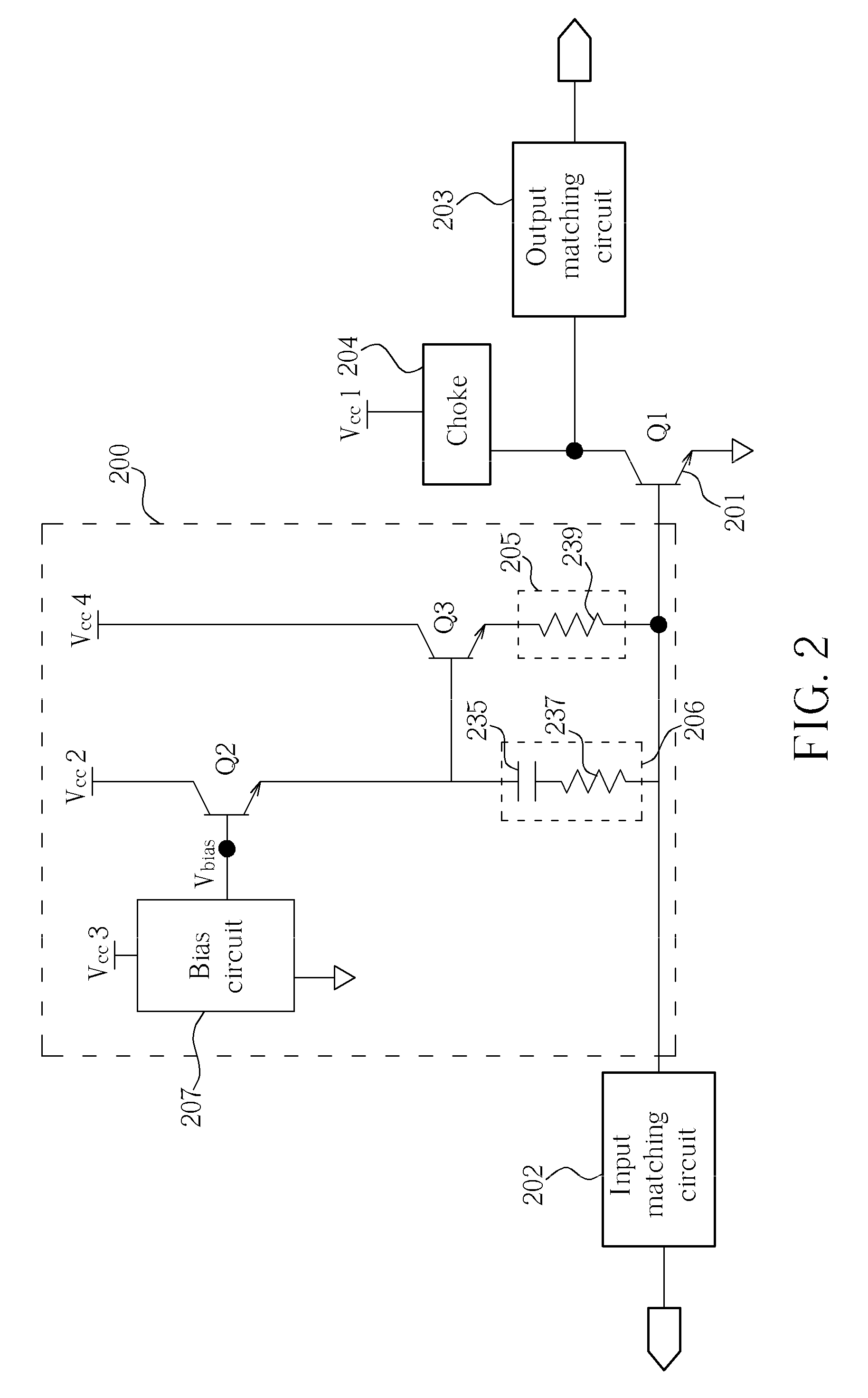
[0022]Please refer to FIG. 2, which is a diagram of an adaptive bias circuit 200 according to the present invention. The adaptive bias circuit 200 biases a power amplifier transistor Q1, which is coupled to a first power supply Vcc1 through a choke 204 and outputs an output signal through an output matching circuit 203. The power amplifier transistor Q1 receives an input signal through an input matching circuit 202 at a base (first terminal, input) of the power amplifier transistor Q1. An emitter (third terminal) of the power amplifier transistor Q1 is coupled to a reference voltage.

[0023]The adaptive bias circuit 200 comprises a bias transistor (first transistor) Q2, a current gain transistor (second transistor) Q3, a bias circuit 207, a first coupling module 206, and a second coupling module 205. A collector (second terminal) of the bias transistor Q2 is coupled to a second power supply Vcc2. An emitter (third terminal) of the bias transistor Q2 is coupled to a base (first termina...


PUM


Abstract

An adaptive bias circuit which provides a more sensitive adaptive bias current with respect to power level is used for biasing an electronic circuit. The adaptive bias circuit has a first transistor coupled to a power supply, a voltage bias circuit coupled to the first transistor and the power supply biasing the first transistor, and a first power coupling module coupled to the first transistor and the electronic circuit for coupling a portion of input signal power to the first transistor. A second transistor is coupled to the first transistor and the power supply to increase the current gain of the adaptive bias circuit, and a second current coupling module is coupled to the second transistor and the electronic circuit to provide adaptive bias current to the electronic circuit.

Description

BACKGROUND OF THE INVENTION[0001]1. Field of the Invention[0002]The present invention relates to an adaptive bias circuit, and more particularly, to an adaptive bias circuit for adaptively biasing a system.[0003]2. Description of the Prior Art[0004]At present, electronic devices are ubiquitous. They can be found in nearly every place imaginable, including the home, the workplace, vehicles, and even our pockets. And, as electronic device technologies mature, for the same cost, the electronic devices become more portable, use less power, and offer greater functionality. In part, this is due to availability of smaller geometry electronic components, such as transistors and on-chip capacitors. However, novel circuit architectures with improved specifications are also responsible for overall performance gains in the electronic devices.[0005]Amplifiers are a key component in practically every electronic device. They vary broadly in their electrical characteristics, such as gain, bandwidth...

Claims


Application Information

Patent Timeline
Patent Type & Authority Patents(United States)
IPC IPC(8): H03F3/04
CPCH03F1/0266H03F1/56H03F3/195H03F3/245H03F2200/555H03F2200/222H03F2200/387H03F2200/451H03F2200/108
Inventor CHEN, CHIH-WEICHAO, CHUAN-JANEWONG, SHYH-CHYI
Owner RICHWAVE TECH CORP
Why Eureka
Try Eureka