Method and apparatus for coupling optical signal with packaged circuits via optical cables and lightguide couplers

a technology of optical cables and couplers, which is applied in the direction of data switching networks, tumbler/rocker switches, instruments, etc., can solve the problems of low voltage networks that cannot be connected to the electrical switching devices within the same wall box, the electrical and building code limitations are delayed, and the photocouplers cannot overcome the limitations of electrical and building codes, etc., to achieve high speed optical communication, reduce overall cost, and reduce the effect of cos

Active Publication Date: 2011-10-18
ELBEX VIDEO LTD
View PDF39 Cites 104 Cited by
  • Summary
  • Abstract
  • Description
  • Claims
  • Application Information

AI Technical Summary

Benefits of technology

[0037]The current drain or the on-off state data is sent in response to the received operational command, such as on-off, or in response to an inquiry command (a request for data) on the basis of the current sensor output, thereby providing error free remote controlling of the electrical home appliances.
[0038]Another object of the present invention is to provide high speed optical communication in homes or offices and the like, by connecting low cost single or dual lightguides or optical fibers directly between two lightguide couplers, including optical communications between communication semiconductor packaged devices that include photo elements and optical links of the present invention, constructed to include optical accesses to lightguides and optical fibers mingled with electrical systems.
[0039]The method of combining a packaged lightguide coupler-AC switching devices and / or current sensor devices with an existing standard electrical switches and outlets, similar to the disclosures in the pending US patent applications, offer several major advantages; one is the lowering of the overall cost of the combined remotely controlled switches and outlets, because standard low cost, mass produced switches and outlets can be used. The second advantage is achieved by joining a lightguide coupler semiconductor packaged switch with a manual switch. The combined joint “lightguide controlled and manually operated switch” can be directly structured onto a packaged lightguide coupler semiconductor switch or they can be joint by plug-in or via screw attachment or otherwise to provide dual operation, manual operation via the commonly used switches and outlets on one hand and remote operation, in parallel with the manual operation, via the lightguide coupler packaged switch. These advantages are the other objects of present invention, attained in total harmony and with no conflict between the manual and remote switching operation as described in the pending US applications.

Problems solved by technology

Low voltage network cannot be connected to the electrical switching device within the same wall box.
The codes however delayed the introduction of low cost simple solutions for automated switching and controlling of electrical appliances and lights.
Even though the input and the output of a photocoupler are electrically insulated, such photocouplers do not overcome the electrical and building codes limitations because the input and the output terminals of the photocoupler devices need to be hard wired and such wires or connections cannot be introduced along side or together with the AC electrical wiring systems of buildings and factories in the advanced countries of the world.
However the lightguide solution disclosed in the above U.S. patent application Ser. No. 12 / 236,656 teaches the use of photo transistor and / or pin diode along with other circuits for providing one or two way communication between a controller and a switch, a relay or a dimmer device, involving number of parts and components assembled into a small packaged device that add to the manufacturing cost.
the light or IR reaching the optical receiver, and therefore reduces the sensitivity, the response time and increase the noise susceptibility.

Method used


Image

  • Method and apparatus for coupling optical signal with packaged circuits via optical cables and lightguide couplers
  • Method and apparatus for coupling optical signal with packaged circuits via optical cables and lightguide couplers
  • Method and apparatus for coupling optical signal with packaged circuits via optical cables and lightguide couplers

Examples


Embodiment Construction

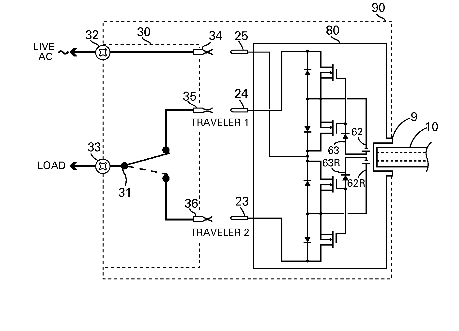
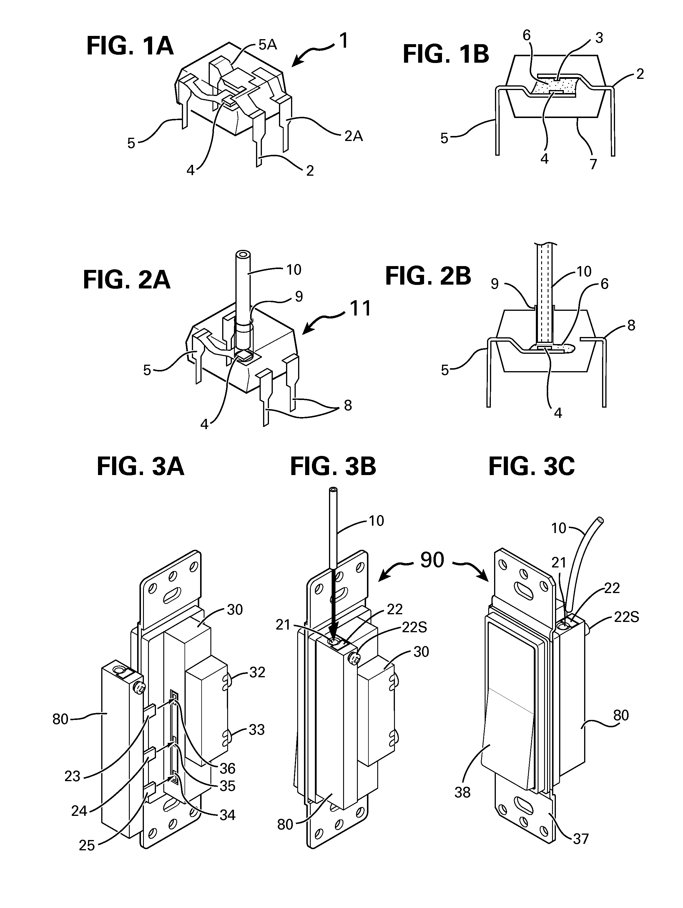
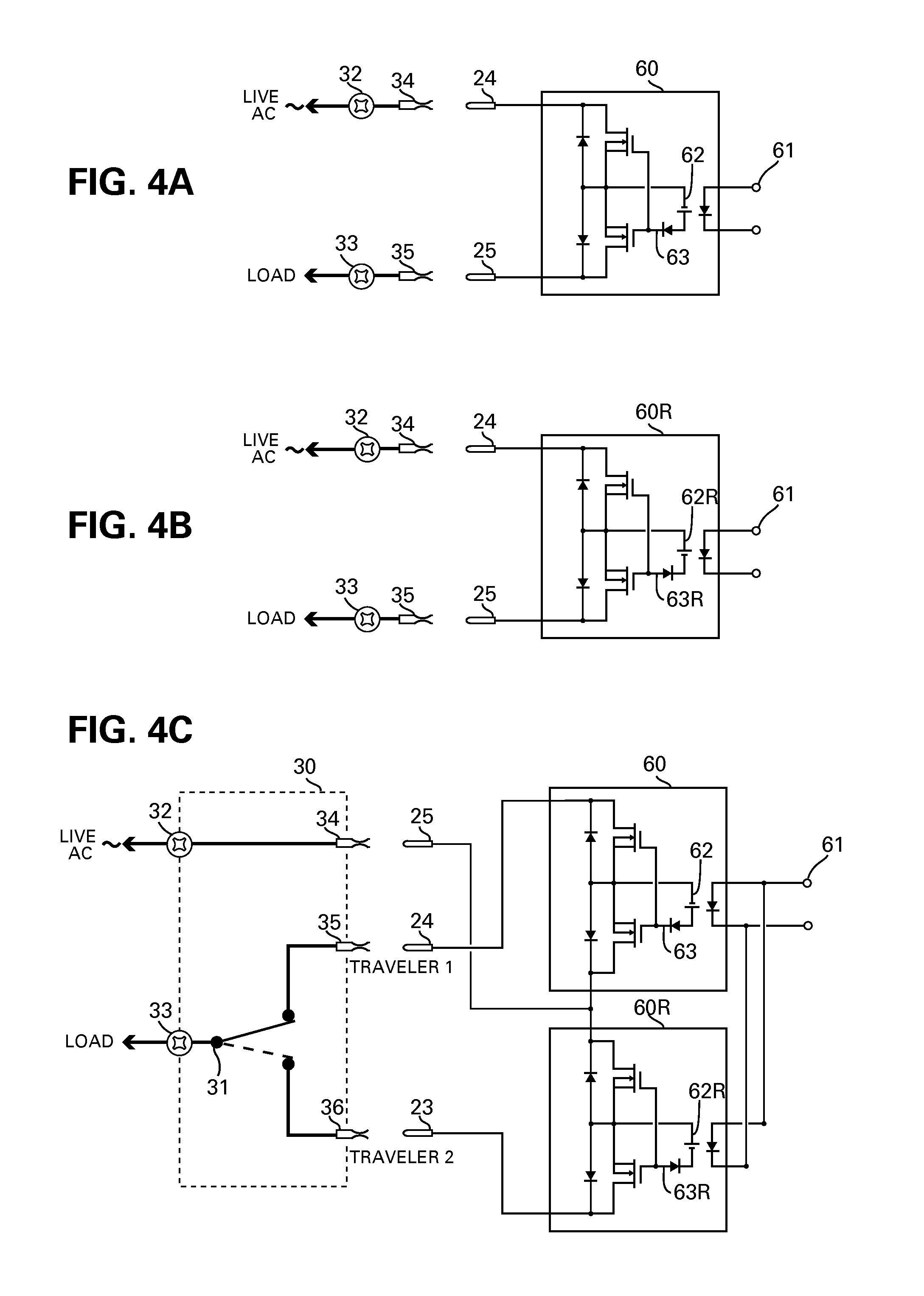
[0070]FIG. 1A shows a typical photocoupler 1 comprising a light transmitter, such as LED 3 of FIG. 1B and a light receiver, such as photo transistor 4 with both the transmitter and the receiver facing each other surface and are optically centered. The transmitter 3 (LED) is connected to and supported by the terminals 2 and 2A and the receiver 4 is connected to and supported by the two terminals 5 and 5A. The input terminals 2 and 2A of the photcoupler 1 are used for receiving electrical input signal and the output terminals 5 and 5A are used for outputting an optical insulated electrical signal. The photocoupler 1 is packaged in a plastic enclosure 7 shown in FIG. 1B. The LED is shown positioned on the upper side and the photo transistor is shown at the bottom side, but this setup can be reversed, or both can be mounted vertically to left and right side of the photocoupler package 7.

[0071]FIG. 1B shows a cross section of the photocoupler structure and the material 6 filling the spac...


PUM


Abstract

Method and apparatus for coupling electrical and communication circuits, included in a packaged semiconductor comprising photo receivers, photo transmitters and photovoltaic cells, through lightguide and optical fiber cables. The packaged semiconductor combinations comprise one, two or plurality of photo elements for a single or plurality one way optical signal, receive or transmit, and a single or plurality of two way optical signal communications via direct optical links and via optical prisms, filters, half mirrors and lenses. The packaged semiconductor includes at least one optical access to a single or plurality of lightguides or optical fiber with single core and for multicore lightguides. A built-in or attachable holders are used for attaching the different lightguide cables to the one or plurality of optical accesses with the attached cable end is terminated by cutting, trimming and shaping. The packaged circuit comprising electrical switches, current sensors, basic elements such as diodes, transistors and FETs, switches and power switches and different basic electrical circuit and communication, distribution circuits including CPU, DSP and complex semiconductor circuits, as used for communicating within limited short distances through optical network of lightguides and fiber optical cables. A packaged semiconductor of an SPDT power switch circuit is integrated with an SPDT manually activated switch, for providing dual switching for lights and other electrical appliances, via manual action and remotely via the lightguide or the optical fiber.

Description

BACKGROUND OF THE INVENTION[0001]1. Field of the Invention[0002]This invention is related to propagation and / or feeding of optical signals via lightguide and plastic optical fibers to a photovoltaic and photocoupler devices comprising switches, MOSFET, transistors, thyristors, triacs and photo relays for use with electrical and communication devices and appliances of home, office and factory automation and communications medium.[0003]2. Description of the Prior Art[0004]Wired or wireless control devices are used for remotely operating AC or DC powered electrical devices and appliances such as heaters, air conditioners, motors and motorized devices, lighting and other electrical appliances in homes, apartments, offices, factories and buildings in general to switch the appliances on-off.[0005]The switching and relay devices that are available for switching appliances on-off and / or for setting or commanding operation levels, such as dimming the lights via triacs or FET switches or via ...

Claims


Application Information

Patent Timeline
Patent Type & Authority Patents(United States)
IPC IPC(8): H04B10/00
CPCG02B6/3817G02B6/4295H04L12/40013H01H9/0271H01H23/168H01L31/167H01L31/173G02B6/02033G02B6/3644G02B6/4292H01H23/24G02B6/4466G02B6/475G02B6/42
Inventor ELBERBAUM, DAVID
Owner ELBEX VIDEO LTD
Why Eureka
Try Eureka