Delay element with a perturber displaceable between first and second microstrip circuits

a technology of perturber and microstrip circuit, which is applied in the direction of waveguides, electrical devices, waveguide types, etc., can solve the problems of actuators that are not sufficiently reliable for continuous operation, return loss, power loss, phase shift, delay,

Active Publication Date: 2011-12-06
PIRELLI & C
View PDF26 Cites 0 Cited by
  • Summary
  • Abstract
  • Description
  • Claims
  • Application Information

AI Technical Summary

Benefits of technology

[0016]Additionally, most of the prior art arrangements discussed in the foregoing use a piezoelectric actuator (i.e., a “bender”) to move the perturber While useful for static operation, such an actuator is not sufficiently reliable for continuous operation and, in general, in those operating scenarios where mechanical stress to the actuator is a limiting parameter for electromechanical devices. Mechanical stress, which strongly limits the useful lifetime and reliability of the actuator, arises whenever moving parts are subjected to strong accelerations. Mechanical stress also depends on the mass (weight) of moving part(s) such as the perturber. In particular, mechanical stress increases when any of the frequency of operation, the mass of the moving part(s), and / or the perturber excursion is increased and / or when speed is abruptly changed during excursion While frequency is determined by the specific application envisaged, device design should maximize inserted time delay, while at the same time reducing excursion and dimensions and weight of moving parts, and avoiding high frequency components in the frequency spectrum of temporal excursion.
[0020]provides satisfactory results in terms of return loss, power losses, delay, and power handling capability, i.e. does not exhibit high RF losses and is able to support high levels of RF power, even at a few GHz and below;
[0021]is thoroughly reliable for fast, continuous operation, with practically no limitations in terms of switching events;
[0046]By providing a second microstrip circuit such an arrangement becomes a tunable, differential delay line, in which the perturber is brought alternatively closer to one microstrip and farther from the other microstrip circuits. As a result, the perturber alternatively accelerates the electromagnetic signals in one microstrip circuit and, at the same time, slows down the electromagnetic signals in the other microstrip circuit, thus enhancing the perturbation effect with respect to single-substrate configuration. In comparison with a single-substrate configuration, the arrangement described herein leads to reduced complexity in the microstrip design and a lower displacement being required for the perturber. This in turn renders less demanding the requirements on linear actuators, which have heretofore represented a major technical limitation in the practical implementation of this kind of device. Moreover, by judiciously selecting the geometric and electromagnetic parameters, the delay element described herein can operate in a linear (or quasi-linear) region of its delay vs. perturber displacement characteristics of the perturber, enabling a simplified control of the device.

Problems solved by technology

The Applicants have observed a number of disadvantages that inevitably militate against the possibility of adopting in a fully satisfactory manner any of the prior art arrangements discussed in the foregoing.
For instance, several of the arrangements considered in the foregoing fail to provide satisfactory results in terms of return loss, power losses, phase-shift, delay, and power handling capability.
Additionally, most of the prior art arrangements discussed in the foregoing use a piezoelectric actuator (i.e., a “bender”) to move the perturber While useful for static operation, such an actuator is not sufficiently reliable for continuous operation and, in general, in those operating scenarios where mechanical stress to the actuator is a limiting parameter for electromechanical devices.
Mechanical stress, which strongly limits the useful lifetime and reliability of the actuator, arises whenever moving parts are subjected to strong accelerations.
In those arrangements that use a rotary disk as the perturber, an arbitrary temporal delay function Δdiff(t) is intrinsically difficult to obtain: this in fact requires changing the rotational speed of the perturber disk, thus imposing very strong stresses on the motor of the disk.

Method used


Image

  • Delay element with a perturber displaceable between first and second microstrip circuits
  • Delay element with a perturber displaceable between first and second microstrip circuits
  • Delay element with a perturber displaceable between first and second microstrip circuits

Examples


Embodiment Construction

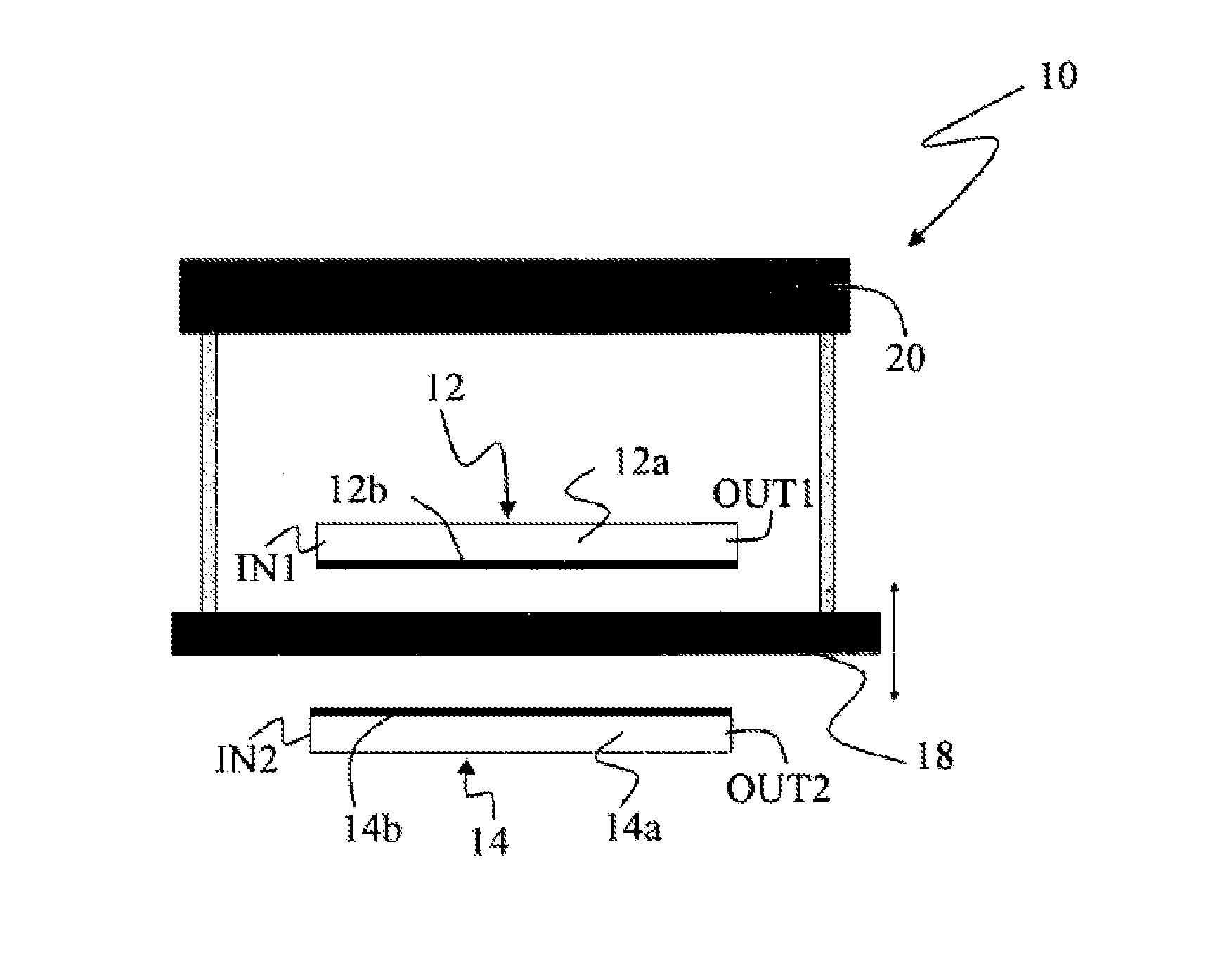
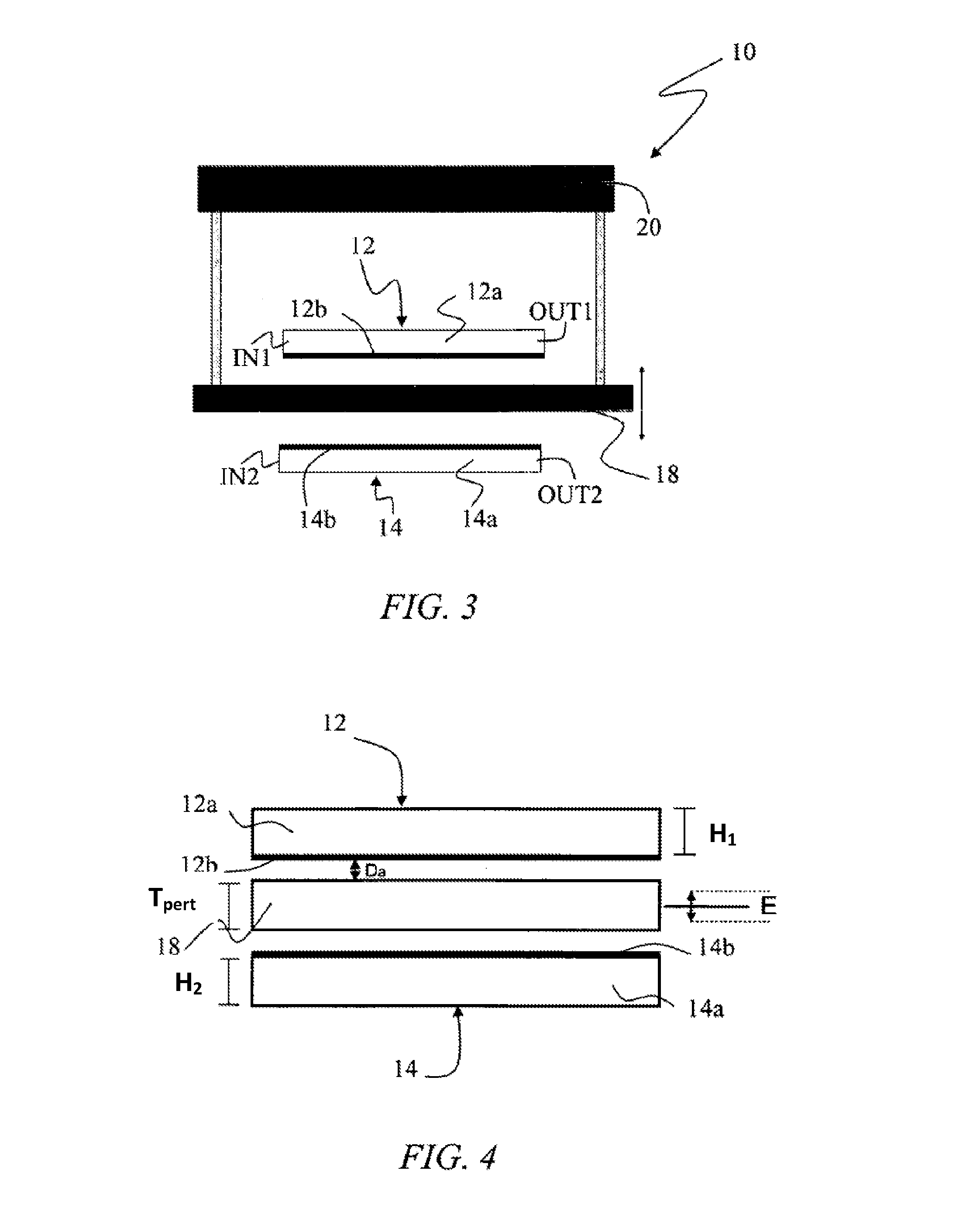
[0058]In FIG. 1, reference 10 denotes as a whole a delay element suitable for operating on electromagnetic signals e.g. in the radio-frequency (RF) and microwave (MW) ranges.

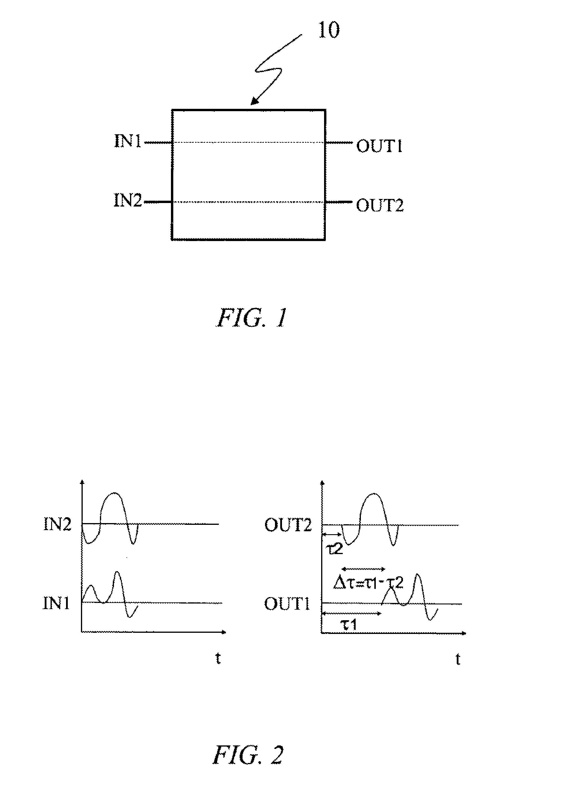
[0059]The element 10 of FIG. 1 is a differential tunable delay line (DTDL), that is a four-port device having two input ports (IN1 and IN2) and two output ports (OUT1 and OUT2). The input port IN1 is connected to the output port OUT1 and the input port IN2 is connected to the input port OUT2.

[0060]In operation, two input electromagnetic signals (e.g. P1 and P2 in FIG. 7) feed the two input ports IN1, IN2 of the device 10 of FIG. 1 and exit from the two output ports OUT1, OUT2. As shown in FIG. 2, the element / device 10 applies a first, time-variable time delay τ1 to the electromagnetic signal input through IN1 and output from OUT1 and a second, time-variable time delay τ2 to the electromagnetic signal that input through IN2 and output from OUT2.

[0061]As a result of passing through the delay device 10, the electro...


PUM


Abstract

A differential delay element for use, e.g., in selectively delaying RF signals in telecommunication systems includes a first microstrip circuit and a second microstrip circuit arranged side-by-side in a facing relationship. The first microstrip circuit defines a first delayed travel path for a first signal from a first input port to a first output port and the second microstrip circuit defines a second delayed travel path for a second signal from a second input port to a second output port. A perturber is arranged between the first and second microstrip circuits, displaceable toward and away from the first and second microstrip circuits, so that when the distance of the perturber to one of the microstrip circuits increases, the distance of the perturber to the other of the microstrip circuits decreases and viceversa. The position of the perturber between the first and second microstrip circuits defines the differential delay, namely the difference (Δτ=τ1−τ2) between the times (τ1,τ2) experienced by the two signals in travelling their travel paths through the delay device.

Description

CROSS REFERENCE TO RELATED APPLICATION[0001]This application is a national phase application based on PCT / EP2006 / 011498, filed Nov. 30, 2006, the content of which is incorporated herein by reference.FIELD OF THE INVENTION[0002]The invention relates to delay elements for use e.g. in telecommunication systems.DESCRIPTION OF THE RELATED ART[0003]Conventional technologies for producing delay elements for use in signal processing e.g. in telecommunication systems include, among other technologies, dielectrically perturbed microstrip delay lines. Perturbation of an electromagnetic field obtained by moving a dielectric or metallic “perturber” is thus the basic principle underlying operation of a variety of delay devices discussed in the technical literature.[0004]For instance, Tae-Yeoul Yun and Kai Chang: “A Low-loss Time-Delay Phase Shifter Controlled by Piezoelectric Transducer to Perturb Microstrip Line”, IEEE MICROWAVE AND GUIDED WAVE LETTERS, VOL. 10, NO, 3, MARCH 2000, pages 96-98, d...

Claims


Application Information

Patent Timeline
Patent Type & Authority Patents(United States)
IPC IPC(8): H01P1/18
CPCH01P5/184H01P9/00
Inventor GRASSANO, GIUSEPPEBOFFA, VINCENZOGATTI, FABRIZIORISI, LUCARUSCITTO, ALFREDOSEMENZATO, PAOLO
Owner PIRELLI & C
Why Eureka
Try Eureka