Methods of forming thin-film transistor display devices

a thin-film transistor and display device technology, applied in semiconductor devices, instruments, optics, etc., can solve the problems of reducing the maximum viewing angle of the display, increasing the delay of rc, and using chromium (cr) as the second metal layer may not be preferred as data line material, etc., to improve the electrode and display characteristics, reduce the resistance contact, and reduce the effect of parasitic metal migration

Inactive Publication Date: 2005-07-21
SAMSUNG ELECTRONICS CO LTD
View PDF15 Cites 4 Cited by
  • Summary
  • Abstract
  • Description
  • Claims
  • Application Information

AI Technical Summary

Benefits of technology

[0012] It is another object of the present invention to provide thin-film transistor display devices which are less susceptible to parasitic metal migration, and methods of forming same.
[0013] It is still another object of the present invention to provide thin-film transistor display devices having improved electrode and display characteristics, and methods of forming same.
[0014] These and other objects, features and advantages of the present invention are provided by thin-film transistor display devices having improved composite electrodes which provide, among other things, low resistance contacts and paths for electrical signals and are less susceptible to parasitic metal migration which can limit display quality and lifetime, and methods of forming same. In particular, a thin-film transistor (TFT) display device is provided having an insulated gate electrode on a face of a substrate (e.g., transparent substrate) and a semiconductor layer on the insulated gate electrode, opposite the face of the substrate. Spaced apart source and drain electrodes are also provided on the semiconductor layer. These source and drain electrodes each preferably comprise a composite of at least two layers containing respective metals therein of different element type. Preferably, one of the layers comprises a metal which is capable of forming a low resistance contact with electrodes such as a pixel electrode (e.g., transparent indium-tin-oxide electrode) and the other of the layers comprises a relatively low resistance metal so that the overall effective resistance of each composite electrode is maintained at a low level.

Problems solved by technology

Unfortunately, the use of chromium (Cr) as the second metal layer may not be preferred as a data line material because it typically has a relatively high resistivity.
This relatively high resistivity can lead to an increased RC delay associated with the data line and can reduce the maximum viewing angle of the display.
The use of chromium as the second metal layer may also be limited by the frequency of formation of metal line discontinuities during processing which can reduce device yield.
Also, the use of aluminum (Al) or an alloy thereof may not be preferred because contact formation between aluminum based alloys and indium-tin-oxide (ITO) layers typically results in the formation of aluminum oxide clusters.

Method used


Image

  • Methods of forming thin-film transistor display devices
  • Methods of forming thin-film transistor display devices
  • Methods of forming thin-film transistor display devices

Examples


Embodiment Construction

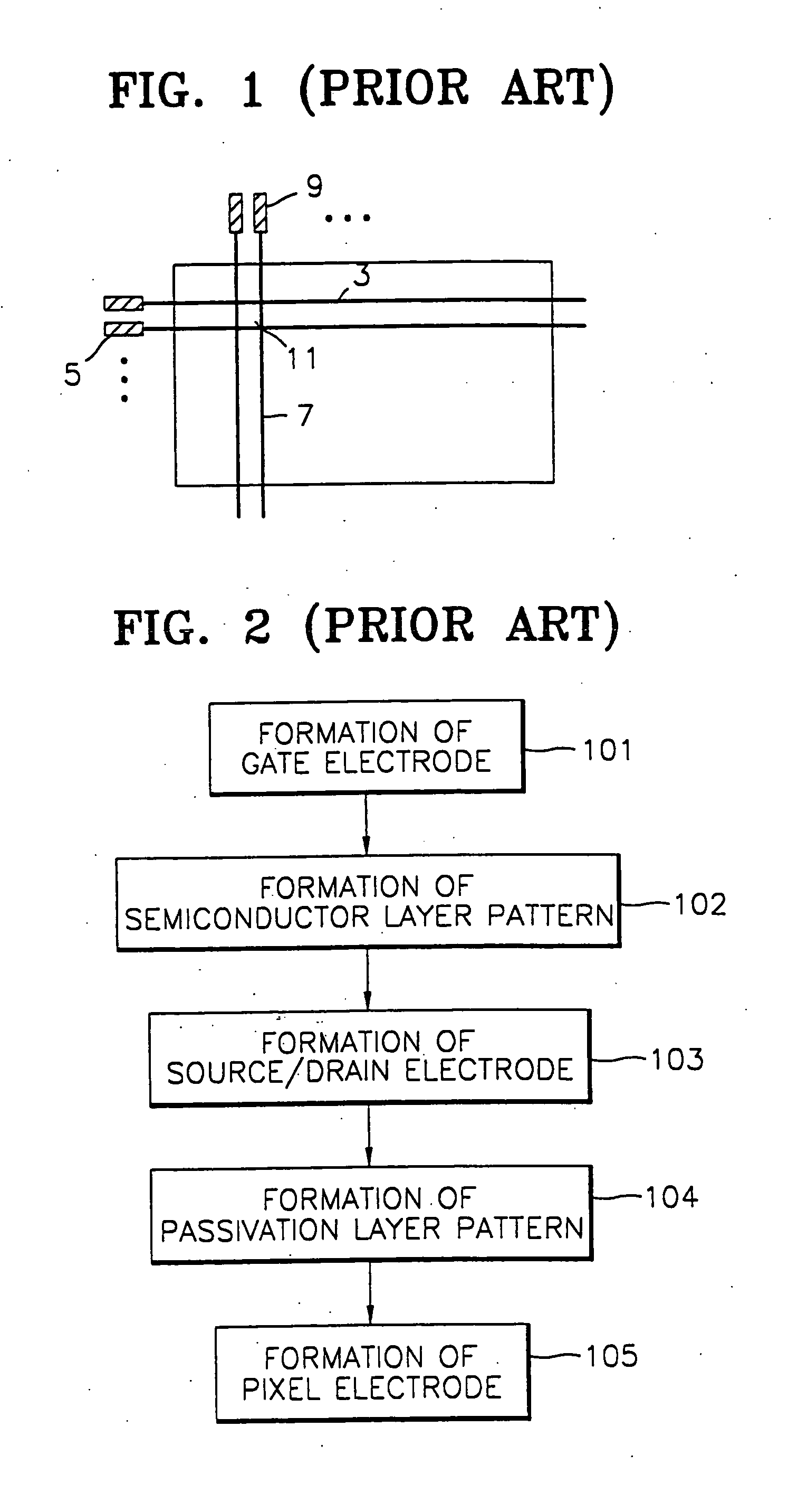
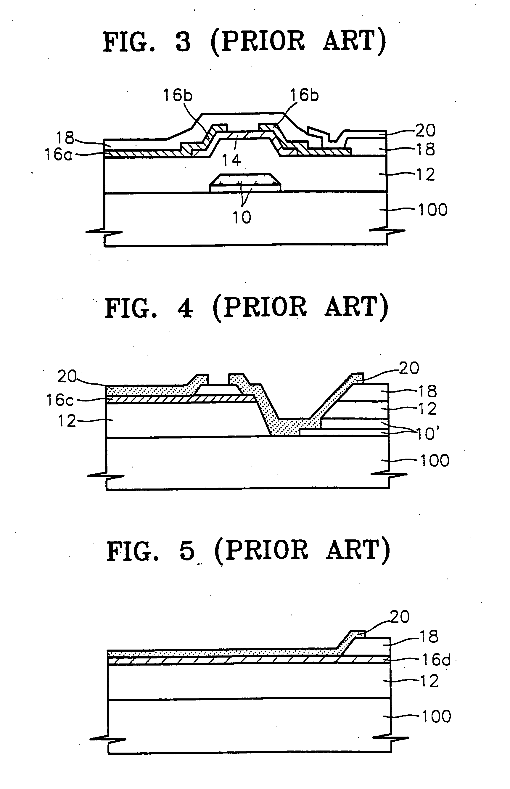
[0024] The present invention will now be described more fully hereinafter with reference to the accompanying drawings, in which preferred embodiments of the invention are shown. This invention may, however, be embodied in different forms and should not be construed as limited to the embodiments set forth herein. Rather, these embodiments are provided so that this disclosure will be thorough and complete, and will fully convey the scope of the invention to those skilled in the art. In the drawings, the thickness of layers and regions are exaggerated for clarity. Like numbers refer to like elements throughout.

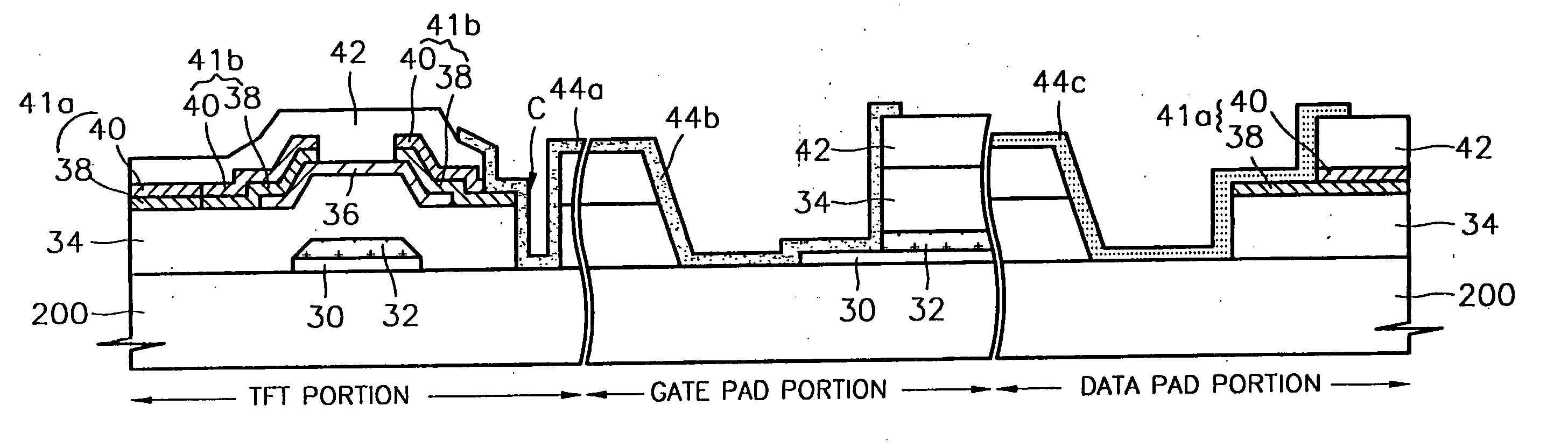
[0025] Referring now to FIGS. 6-8, a thin-film transistor display device according to a first embodiment of the present invention will now be described. Here, FIGS. 6-8 illustrate cross-sectional views of portions of an integrated thin-film transistor display device, including a thin-film transistor portion, a gate pad portion and a data pad portion, respectively. In particular,...


PUM

PropertyMeasurementUnit
conductiveaaaaaaaaaa
semiconductoraaaaaaaaaa
conductivityaaaaaaaaaa

Abstract

Methods of forming thin-film transistor display devices including forming a gate line and a gate electrode on a face of a substrate and forming a semiconductor layer that is insulated from the gate line. A data line and a source / drain electrode are formed on the semiconductor layer. The data line and the source / drain electrode are formed as composites of at least two different metal conductive layers. A transparent pixel electrode is formed that is electrically coupled to the drain electrode.

Description

REFERENCE TO PRIOR-FILED APPLICATIONS [0001] This application is a continuation of U.S. application Ser. No. 10 / 406,668, filed Apr. 3, 2003, now U.S. Pat. No. ______, which is a divisional of U.S. application Ser. No. 10 / 092,282, filed Mar. 6, 2002, now U.S. Pat. No. 6,566,686, which is a continuation of U.S. application Ser. No. 09 / 770,576, filed Jan. 26, 2001, now U.S. Pat. No. 6,383,831, which is a divisional of U.S. application Ser. No. 08 / 808,886, filed Feb. 28, 1997, now U.S. Pat. No. 6,087,678, the disclosures of which are hereby incorporated herein by reference.FIELD OF THE INVENTION [0002] The present invention relates to display devices and methods of fabrication, and more particularly to liquid crystal display devices and methods of fabricating liquid crystal display devices. BACKGROUND OF THE INVENTION [0003] In order to minimize the space required by display devices, research into the development of various flat panel display devices such as LCD display devices, plasma ...

Claims


Application Information

Patent Timeline
Patent Type & Authority Applications(United States)
IPC IPC(8): G02F1/136H01L21/336H01L29/417H01L29/45
CPCG02F1/13458G02F1/136227G02F1/136286G02F2001/13629H01L27/124H01L29/41733H01L29/458H01L29/66765H01L27/12G02F1/13629G02F1/136
Inventor KIM, DONG-GYU
Owner SAMSUNG ELECTRONICS CO LTD
Why Eureka
Try Eureka