
Waveguide connecting structure

a technology of connecting structure and waveguide, applied in the direction of optical waveguide light guide, instruments, optics, etc., can solve the problem that the conventional techniques described above cannot be applied to the connection to a slot waveguid

Active Publication Date: 2011-12-13
NEC CORP
View PDF11 Cites 9 Cited by
  • Summary
  • Abstract
  • Description
  • Claims
  • Application Information

AI Technical Summary

Benefits of technology

The present invention provides a waveguide connecting structure that can connect a conventional optical waveguide to a slot waveguide including two waveguides arranged in parallel at a narrow spacing. This structure includes a light branching element and a twin-arm waveguide with a high refractive index core. The light branching element branches light from an input optical waveguide into two branched light components with the same power and phase. The twin-arm waveguide has a narrowing spacing between its arm waveguides and is designed to match the spacing of the slot waveguide. This structure allows for efficient coupling of optical signals between the conventional and slot waveguides.

Problems solved by technology

Unfortunately, the conventional techniques as described above cannot be applied to the connection to a slot waveguide, because the connecting structures as objects of research and development are those of a rib waveguide, ridge waveguide, strip waveguide, and photonic crystal line defect waveguide.

Method used


Image

  • Waveguide connecting structure
  • Waveguide connecting structure
  • Waveguide connecting structure

Examples


first exemplary embodiment

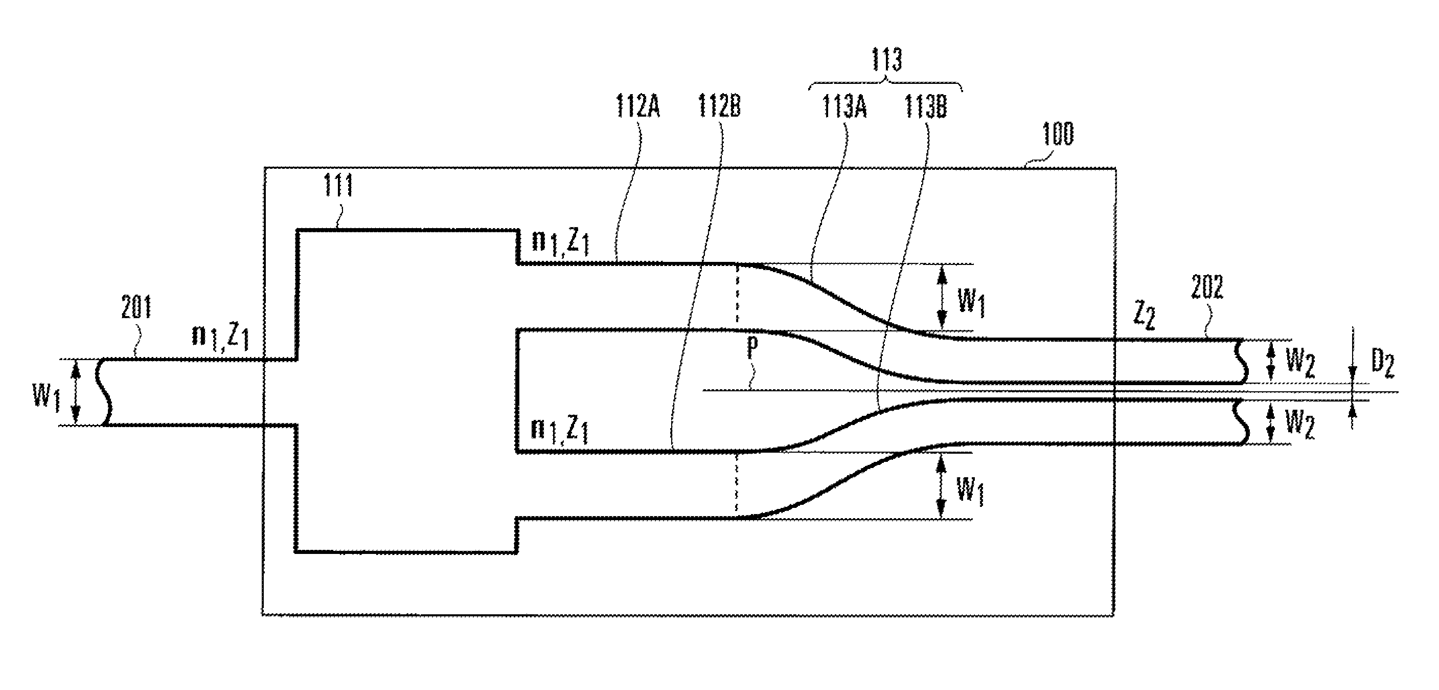
[0040]A waveguide connecting structure according to the first exemplary embodiment of the present invention will be explained below with reference to FIGS. 6A and 6B. FIGS. 6A and 6B are views showing the waveguide connecting structure according to the first exemplary embodiment of the present invention. FIG. 6A is a plan view, and FIG. 6B is a front view.

[0041]A waveguide connecting structure 100 is a waveguide connecting structure connecting an input optical waveguide (strip waveguide) 201 including one core and a slot waveguide 202 including two cores arranged in parallel at a narrow spacing D2. The waveguide connecting structure 100 includes an MMI (Multi-mode Interference) element 111, strip waveguides 112A and 112B, and a twin-arm waveguide 113.

[0042]The MMI element 111 is an optical element having a function of branching an electromagnetic field mode passing through the input waveguide 201 into the two strip waveguides 112A and 112B at an optical power branching ratio of 50:5...

second exemplary embodiment

[0056]A waveguide connecting structure according to the second exemplary embodiment of the present invention will be explained below with reference to FIGS. 10A and 10B. FIGS. 10A and 10B are plan views showing the waveguide connecting structure according to the second exemplary embodiment of the present invention, in which the same reference numerals as in FIGS. 6A and 6B denote the same parts or similar parts.

[0057]The first exemplary embodiment has been explained by taking the case in which the MMI element 112 branches light from the input waveguide 201 as an example. This exemplary embodiment will be explained by taking the case in which a Y light branching element 115 branches light from an input waveguide 201 as an example.

[0058]In a waveguide connecting structure 101, the Y light branching element 115 is an optical element having a function of branching an electromagnetic field mode passing through the input waveguide 201 to two strip waveguides 112A and 112B at a power branc...


PUM


Abstract

A waveguide connecting structure includes a light branching element (111) for branching light from an input optical waveguide (201) including one core into two branched light components having the same optical power and the same phase, and a twin-arm waveguide (113) including a pair of arm waveguides (113A, 113B) for outputting the light components branched by the light branching element to a slot waveguide (202) including two cores arranged in parallel at a narrow spacing. The pair of arm waveguides have cores formed in a cladding on a substrate and having a refractive index higher than that of the cladding, and are formed such that the spacing between them gradually narrows and becomes equal to the core spacing of the slot waveguide from the core input ends into which the branched light components enter toward the core output ends from which the light components are output to the slot waveguide.

Description

[0001]This application is the National Phase of PCT / JP2007 / 073941, filed Dec. 12, 2007, which is based upon and claims priority from Japanese Patent Application No. 2006-351587 filed Dec. 27, 2006.TECHNICAL FIELD[0002]The present invention relates to a connecting structure between dissimilar waveguides in a micro-optical circuit and, more particularly, to a connecting structure from a strip waveguide to a slot waveguide.BACKGROUND ART[0003]The research and development of micro-optical circuits are being extensively made in optical communication systems using waveform multiplexing. When an optical device using an optical waveguide made of materials having a large refractive index difference is achieved, a lower-cost, lower-power-consumption optical communication apparatus than the conventional apparatuses can be implemented. Also, the developed optical device element technologies are applicable to optical interconnections on an LSI chip or between chips, and expected as means for avo...

Claims


Application Information

Patent Timeline
Patent Type & Authority Patents(United States)
IPC IPC(8): G02B6/26G02B6/42
CPCG02B6/1228G02B6/125G02B6/14G02B2006/12147
Inventor USHIDA, JUN
Owner NEC CORP
Learn More