[0011]A first advantage of the present invention is that both the high intensity of the optical field and the close proximity of the electrodes are exploited, for several purposes. First, detection of optical signals via direct conversion to electrical energy is shown, by means of nonlinear optical rectification. Nonlinear optical rectification is discussed, for example, in reference [7], incorporated herein by reference in its entirety.
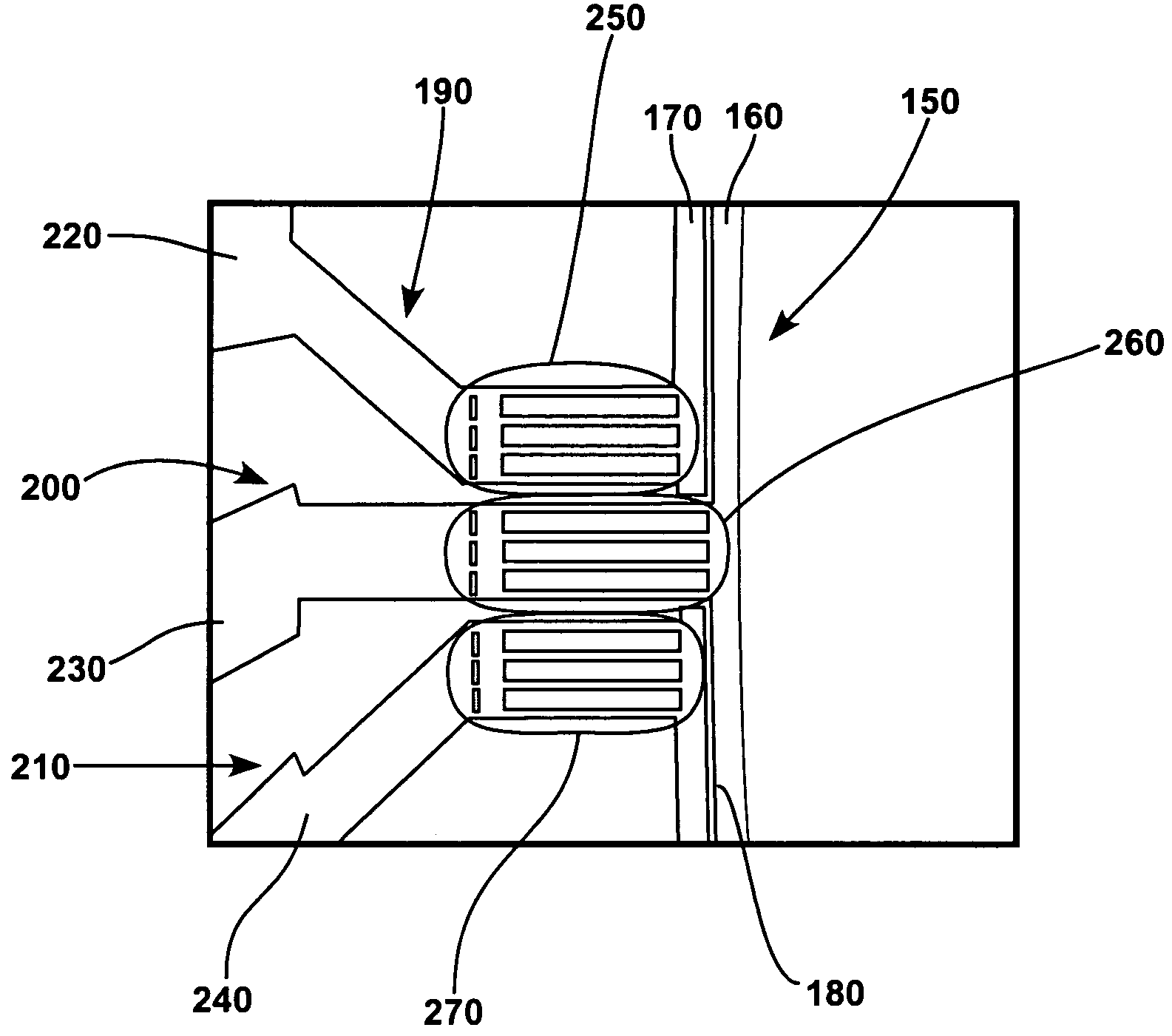
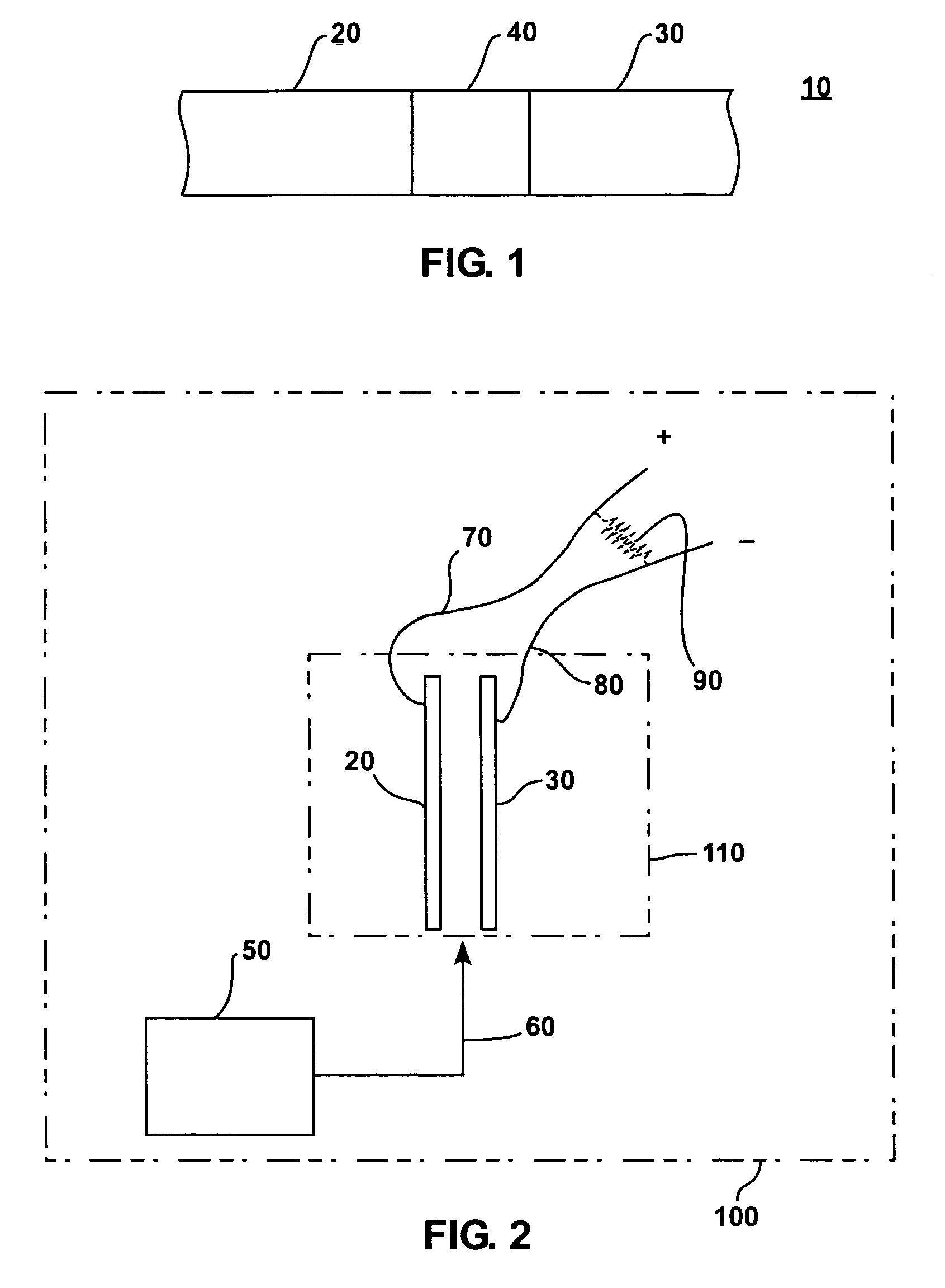
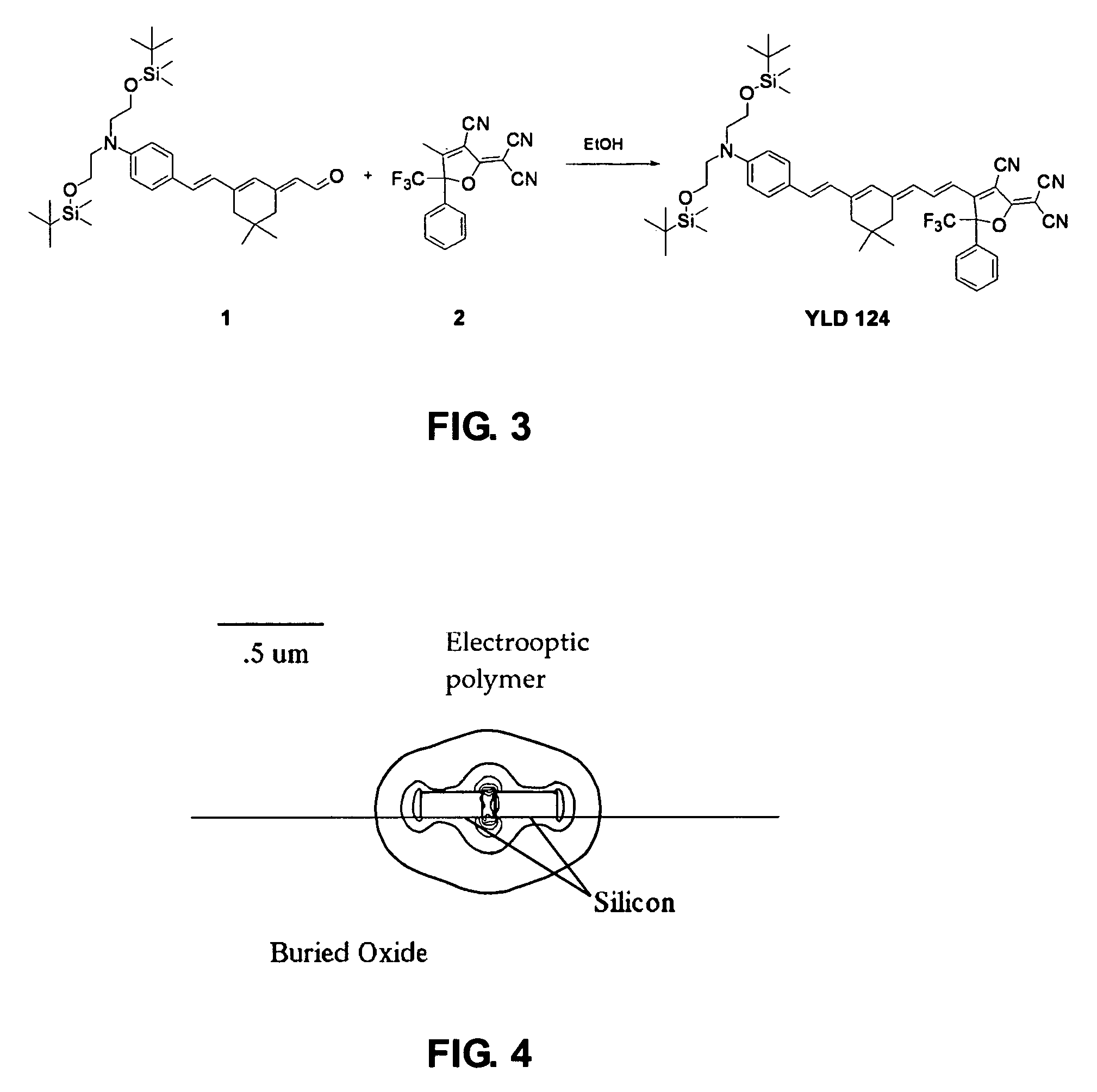
[0012]A device in accordance with the present disclosure comprises a split ring resonator with an electro-optic polymer based χ2 (chi-2) material deposited as a cladding. Materials of this kind are discussed, for example, in [8, 9], both incorporated herein by reference in their entirety. Inside the slot, the high optical field intensity creates a standing DC field, which creates a virtual voltage source between the two electrodes (e.g. silicon electrodes), resulting in a measurable current flow, in the absence of any external electrical bias. One example of such a material is a poled electrooptic polymer. Such a material is deposited in an unordered state, as the orientation of the chromophores in the polymer has no intrinsic order. Such a material can be made to develop a second order (chi-2) nonlinear optical moment through the process of poling. Poling generally consists of heating the material above or near its glass transition temperature, and then a voltage being applied to create an electric field across the polymer. This electric field can be developed from integrated electrodes, or from a field discharged from an emitter tip. In the case of the use of an external emitter tip, the process is generally referred to as ‘corona poling’. In either case, the field on the polymer forces the chromophores into an ordered state; when the temperature of the substrate is reduced below the glass transition, this ordering, and thus the associated second order nonlinear moment, is ‘frozen in’ to the material.
[0013]Though optical rectification has been observed in electro-optic polymers elsewhere (see reference [10], incorporated herein by reference in its entirety), typically instantaneous optical powers on the order of 1 kW are needed for observable conversion efficiencies, often achieved with pulsed lasers. In accordance with the present disclosure, measurable conversion with less than 1 mW of non-pulsed input can be obtained, obtained from a standard, low power tunable laser near 1500 nm.
[0014]Also standard Pockels' effect based modulation (see reference [11], incorporated herein by reference in its entirety) can be obtained, which is similarly enhanced by means of the very small scale of the device according to the disclosure. The close proximity of the electrodes, and ready overlap with the optical mode, causes an external voltage to produce a far larger effective electric modulation field, and therefore refractive index shift, than would be obtained through conventional waveguide designs (see reference [12], incorporated herein by reference in its entirety). The applicants have shown this through the tuning of the resonance frequencies of a slot waveguide ring resonator. Reference can also be made to U.S. application Ser. No. 11 / 280,854 for “Coupled Segmented Waveguide Structures” filed on Nov. 15, 2005, incorporated herein by reference in its entirety.
[0015]By means of the nanoscale slotted waveguide geometry in accordance with the present disclosure, massive enhancements of the optical field have been obtained over what is generally achieved in fibers or in free space optics. That has in turn enabled the applicants to exploit nonlinear optical processes that are typically only available in the kW regime in fibers or free space in the sub-mW regime. This difference is so considerable that the applicants believe it represents a change in kind for the function of nonlinear optical devices; it may be possible to someday construct a practical, low-power detector based on nonlinear optical rectification. In addition, the applicants expect this hybrid material system to provide a means for creating compact devices that exploit other nonlinear phenomena on-chip.
[0016]Optical rectification based detectors might have many advantages over currently available technology. In particular, such detectors would probably be able to function at a higher intrinsic rate than the typical photodiode in use, as the optical rectification process occurs at the optical frequency itself, on the order of 100 THz in WDM systems. The absence of an external bias, and ability to generate a voltage or current source on-chip powered directly by the optical field without the application of any external electrical energy source, may prove to be of great utility. The applicants also do not believe that a device based on nonlinear optical rectification would suffer from the limitation of a dark current. This in turn might mean that current WDM and other optical systems could function with lower optical power, providing numerous benefits. Similarly, presence of enhanced modulation using these waveguide geometries may also lead to useful components in future communications systems.

