Wire-bonding free packaging structure of light emitted diode

a technology of light-emitting diodes and packaging structures, applied in the direction of basic electric elements, electrical apparatus, semiconductor devices, etc., can solve the problems of limited junction breakdown, poor heat transfer, and leds are still difficult to be used in illumination, and achieve good heat transfer and enhanced light intensity

Inactive Publication Date: 2007-10-04
INTEGRATED CRYSTAL TECH
View PDF2 Cites 73 Cited by
  • Summary
  • Abstract
  • Description
  • Claims
  • Application Information

AI Technical Summary

Benefits of technology

[0010] The object of the present invention is to provide a wire-bonding free packaging structure for light emitting diode (LED). A silicon sub mount with a reach-through U-shape cavity is used to accommodate a flip-chip LED, and form a stack-integrated packaging module with solder bump on the surface, the module is then bonded to an aluminum PC board with flip-chip surface mount packaging technology, thus the LED will have very good heat transfer and the light intensity will be enhanced.

Problems solved by technology

However, the light intensity is limited to junction breakdown, which is mostly due to over heating of the junction.
It results not only the route of heat transfer is too long, but also the conduction area of the gold wire is too small, thus results very bad heat transfer.
This is the cause that LED is still difficult to be used in illumination, such as the head light of a car, room illumination, etc.
Thus it is still need a LED light source to replace the electric light bulb or fluorescent lamp with high energy consumption.

Method used


Image

  • Wire-bonding free packaging structure of light emitted diode
  • Wire-bonding free packaging structure of light emitted diode
  • Wire-bonding free packaging structure of light emitted diode

Examples


Embodiment Construction

[0028] The foregoing and other advantages of the invention will be more fully understood with reference to the description of the best embodiment and the drawing as followed description.

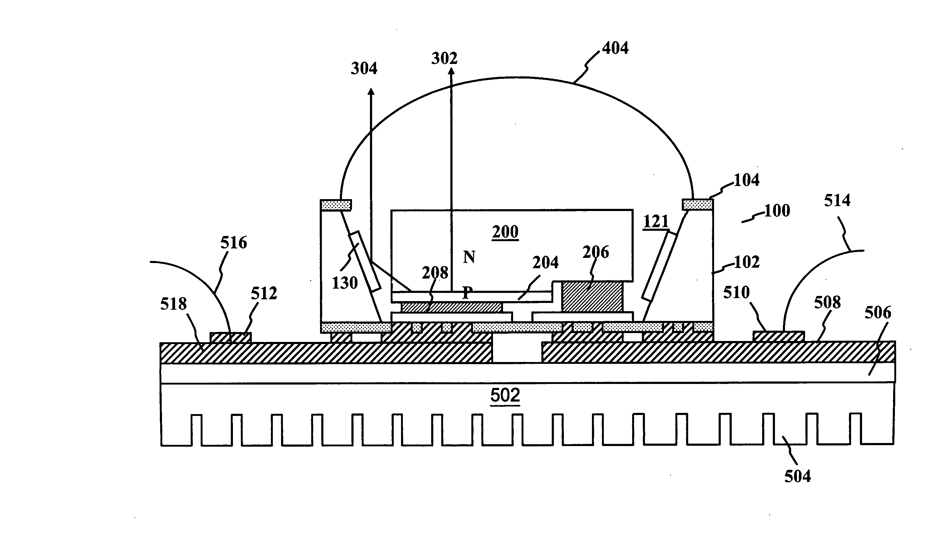
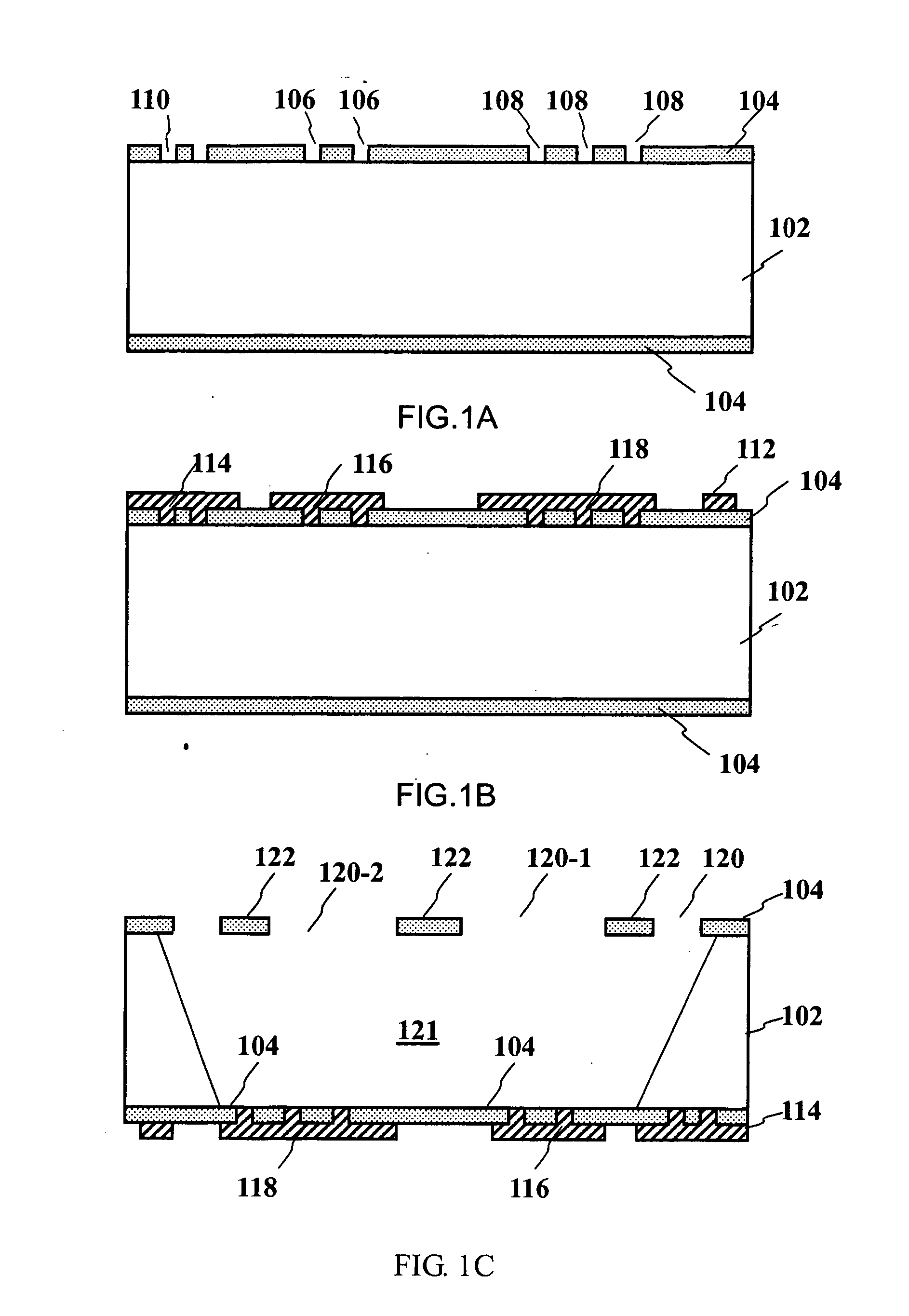
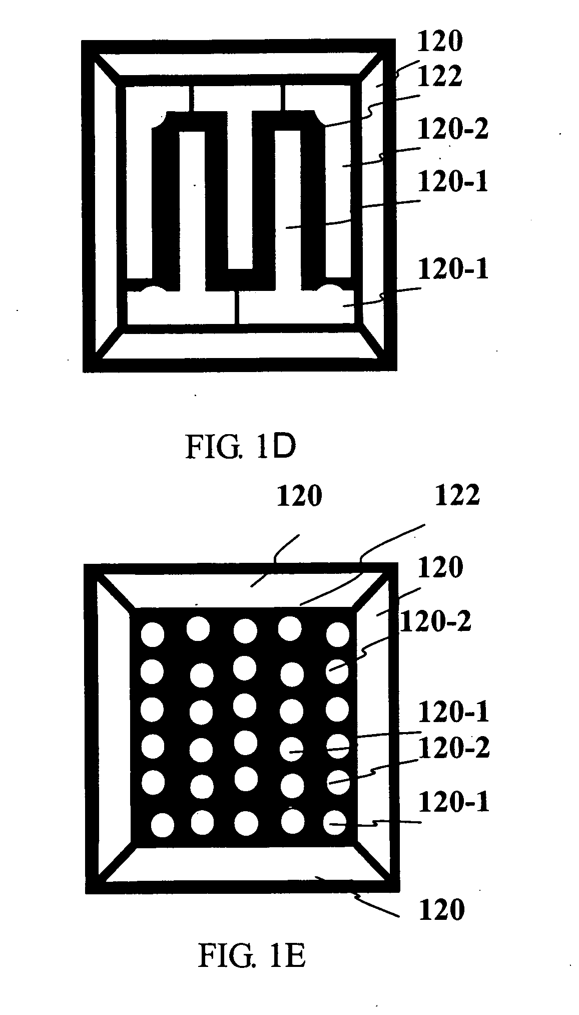
[0029] The manufacturing procedure of the packaging structure in according to the present invention can be understood by referring to FIG. 1 through FIG. 7. FIG. 1 illustrates the manufacturing steps of a silicon sub-mount in according to one embodiment of the present invention. First, as shown in FIG. 1 (A), FIG. 1 (A) is the step of forming an align mark and contact via holes in cross sectional view. Prepare the p-type silicon wafer 102 which is (100) orientation, any doping, even a reclaimed substrate. A layer of silicon nitride 104 is deposited on both sides of the wafer by LPCVD. On the front side, a first mask is used in lithography to form a negative via hole 106, a positive via hole 108 and an align mark for the stepper. Refer to FIG. 1 (B). FIG. 1 (B) is a cross sectional view of the step f...


PUM


Abstract

A wire-bonding free packaging structure for light emitting diode (LED) is provided. Prepare a silicon sub-mount having a backside bulk micromachining reach-through U-shape cavity for accommodating a flip-chip LED. This stack-integrated packaging module with solder bumps on the surface is than bonded to an aluminum PC board with flip-chip surface mount packaging or bump technology. This gives very good heat conduction to the heat sink of the PC board and can endure more current to enhance light intensity of the LED. This stack-integrated packaging module can also be bonded on a lead frame with two leg packaging, which can also increase heat conduction.

Description

BACKGROUND OF THE INVENTION [0001] 1. Field of the Invention [0002] The present invention relates to a packaging structure of light emitting diode (LED). In particular, relates to a wire-bonding free packaging structure for LED mounted into a sub-mount. [0003] 2. Description of the Related Art [0004] As a good light source and device made by III-V or II-VI semiconductor material, LEDs possesses advantages of small size, long life time, low driving voltage, rapid response and good oscillation-proof, etc. [0005] By changing the semiconductor materials and device structure of LEDs, different visible and invisible light can be achieved, wherein AlGaAs, InGaAlP and InGaN are suitable for producing LEDs with high luminance of more than 1000 mcd. [0006] In order to increase the light intensity of a LED, the compound materials used has widely studied, also the structure of the device can be modified such as Double Hetero Junction (DH), quantum well (QW) or multi-quantum wells (MQW), etc., t...

Claims


Application Information

Patent Timeline
Patent Type & Authority Applications(United States)
IPC IPC(8): H01L33/00H01L33/38H01L33/46H01L33/48H01L33/64
CPCH01L33/46H01L33/486H01L2224/16H01L33/62H01L33/64H01L33/60
Inventor SHIE, JIN-SHOWNHSIEH, C.Y.LIN, CHIEN CHUNG
Owner INTEGRATED CRYSTAL TECH
Why Eureka
Try Eureka