Exposure system and method of manufacturing a semiconductor device

a technology of semiconductor devices and manufacturing methods, applied in the field of exposure systems and methods of manufacturing semiconductor devices, can solve the problems of increasing the manufacturing cost of semiconductor devices, increasing the processing time of wafers in the exposure process, and reducing throughput, so as to reduce the processing time of each single wafer and reduce the throughput

Inactive Publication Date: 2011-12-20
GK BRIDGE 1
View PDF15 Cites 0 Cited by
  • Summary
  • Abstract
  • Description
  • Claims
  • Application Information

AI Technical Summary

Benefits of technology

[0019]However, the processing time for each single wafer increases when performing the focus calibration on each wafer immediately prior to exposure thereby reducing the throughput. For example, the time required for the spatial image focus measurement is 30 seconds to 60 seconds, and the time required for exposure processing to expose an integrated circuit pattern to a wafer is also 30 seconds to 60 seconds. In this case, the time required to process a single wafer is twice that compared to not performing the focus calibration immediately before exposing each wafer.
[0021]The present invention has the objective of providing an exposure system and semiconductor device manufacturing method that has the ability to perform exposure by optimizing the focus for each wafer to the best focus without reducing throughput in exposure process of wafers per lot unit.
[0023]According to the present constitution, a focus curve can be obtained with only a single exposure of the spatial image mark body. Therefore, the best focus position of the spatial image can be calculated in an extremely short time.
[0029]According to the present invention, since the focus curve is obtained by a single exposure, the best focus position can be calculated in an extremely short period of time. Therefore, when performing exposure process of substrates per lot unit, the exposure process can be implemented to optimize the focus for each substrate without reducing the throughput. As a result, the focus variance can be controlled between each wafer belonging to the same lot without reducing throughput thereby enabling to reduce in manufacturing cost.

Problems solved by technology

However, the processing time for each single wafer increases when performing the focus calibration on each wafer immediately prior to exposure thereby reducing the throughput.
This increases the manufacturing cost for semiconductor devices.
Therefore, an increase in the wafer processing time is not allowed in the exposure process.
However, since it is a method for deriving the best focus by measuring the resist pattern dimension, the best focus adjustment requires a certain period of time.
Further, since it is not a method for the spatial image focus measurement, implementing immediately prior to exposure on each wafer is difficult.

Method used


Image

  • Exposure system and method of manufacturing a semiconductor device
  • Exposure system and method of manufacturing a semiconductor device
  • Exposure system and method of manufacturing a semiconductor device

Examples


Embodiment Construction

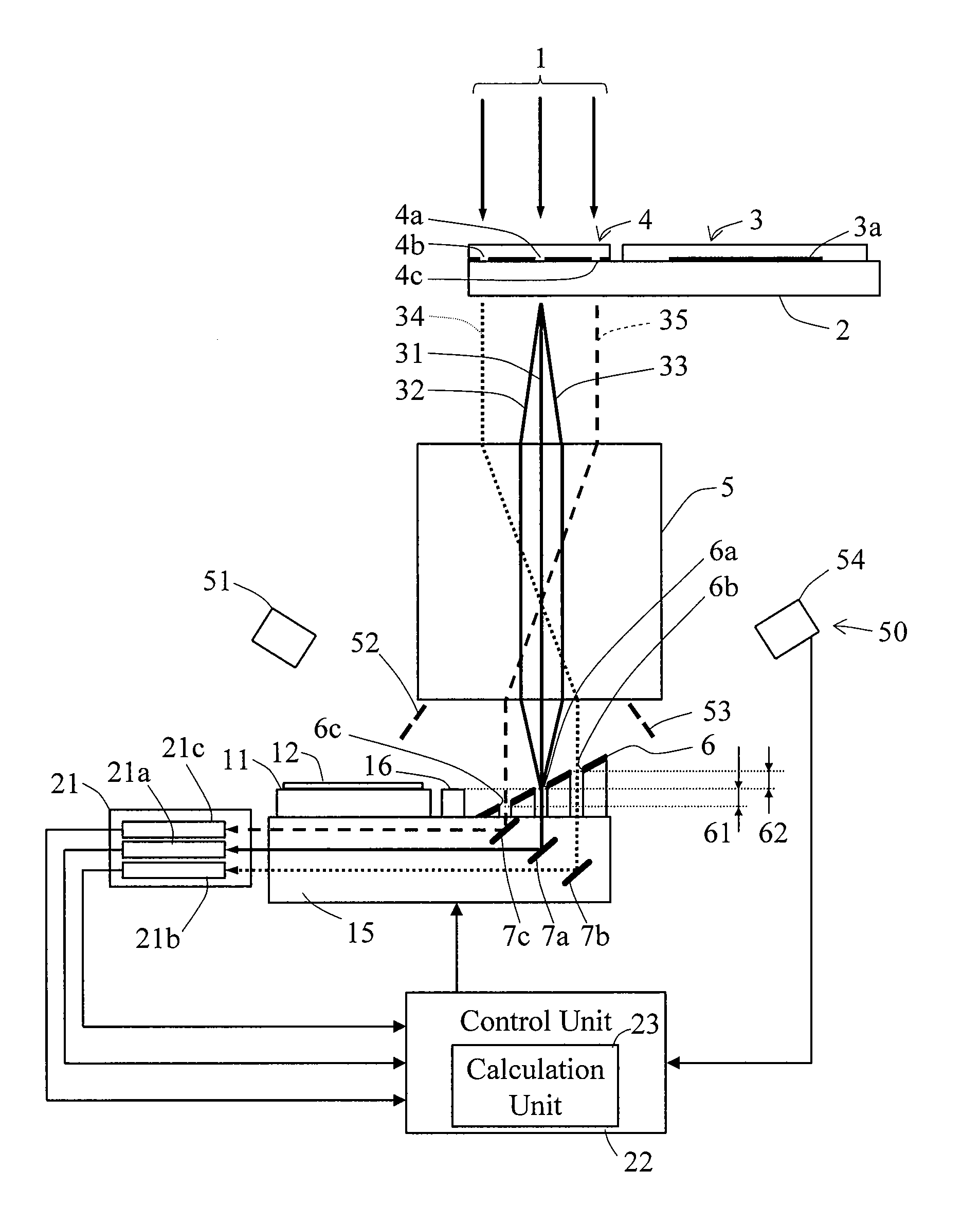
[0036]A detailed description with reference to drawings will be described hereafter of a preferred embodiment of the present invention. A reduction projection exposure apparatus is specifically used in the following preferred embodiment for the present invention.

[0037]FIG. 1 is an outline structural diagram to explain the composition of an exposure apparatus in the embodiment relating to the present invention. As shown in FIG. 1, the exposure apparatus of the present embodiment irradiates an exposure light 1 that exits from an exposure light source (not shown) to a reticle 3 mounted on the reticle stage 2, and an element pattern 3a formed on the reticle 3 undergoes image formation on a wafer 12 through a projection lens 5. The reticle stage 2 is arranged between the exposure light source and the projection lens 5. Further, a spatial image mark body 4 is arranged on the reticle stage 2 and which arranges a plurality of spatial image marks 4a, 4b, and 4c in a same plane. The reticle s...


PUM


Abstract

In an exposure system and semiconductor device manufacturing method relating to the present invention, an image of spatial image mark body through a reduction projection lens is projected onto a spatial image projection plate arranged on a wafer stage by irradiating the spatial image mark body arranged on a reticle stage with an exposure light. The spatial image mark body has a plurality of spatial image marks arranged in a same plane. At projection positions of images of each spatial image mark on the spatial image projection plate, spatial image openings are equipped with differing positions in an optical axis direction of the exposure light. A focus curve with a single exposure can be obtained, without moving the wafer stage in the optical axis direction, by respective measurements of optical intensities of images of each spatial image mark through each opening thereby enabling to calculate the best focus position.

Description

CROSS-REFERENCE TO RELATED APPLICATION[0001]The present application claims the benefit of Japanese Patent Application No. 2007-238981 filed Sep. 14, 2007, the subject matter of which is incorporated herein by reference.BACKGROUND OF THE INVENTION[0002]1. Field of the Invention[0003]The present invention relates to an exposure system used in an exposure process for manufacturing semiconductor devices, etc. and a semiconductor device manufacturing method that includes a step of adjusting each wafer to the best focus by measuring a focus setting value of an exposure apparatus for each wafer when exposure process is performed on a lot-to-lot basis.[0004]2. Description of the Related Art[0005]In a conventional manufacturing process of semiconductor devices such as semiconductor integrated circuits or the like, an exposure apparatus having a large numerical aperture is used to improve a resolution for a micro-sized element pattern. However, as the numerical aperture increases, the allowab...

Claims


Application Information

Patent Timeline
Patent Type & Authority Patents(United States)
IPC IPC(8): G03B27/52G03B27/68G03B27/54G03B27/74G03B27/32G03B27/58
CPCG03F9/7026G03F9/7034G03F7/70425G03F7/70716
Inventor NISHINO, KATSUHIROYOSHIDA, TAKATSUGU
Owner GK BRIDGE 1
Why Eureka
Try Eureka