

Wiring structure of a substrate
a technology of wiring structure and substrate, which is applied in the direction of cross-talk/noise/interference reduction, printed capacitor incorporation, printed electric component incorporation, etc., can solve the problems of reducing the size and profile of the semiconductor substrate, difficult to secure the continuity of a characteristic impedance of the signal wire, and difficult to secure the return path of the return current. achieve the effect of ensuring the transmission quality of high-frequency signals
- Summary
- Abstract
- Description
- Claims
- Application Information
AI Technical Summary
Benefits of technology
Problems solved by technology
Method used
Image

Examples
embodiment
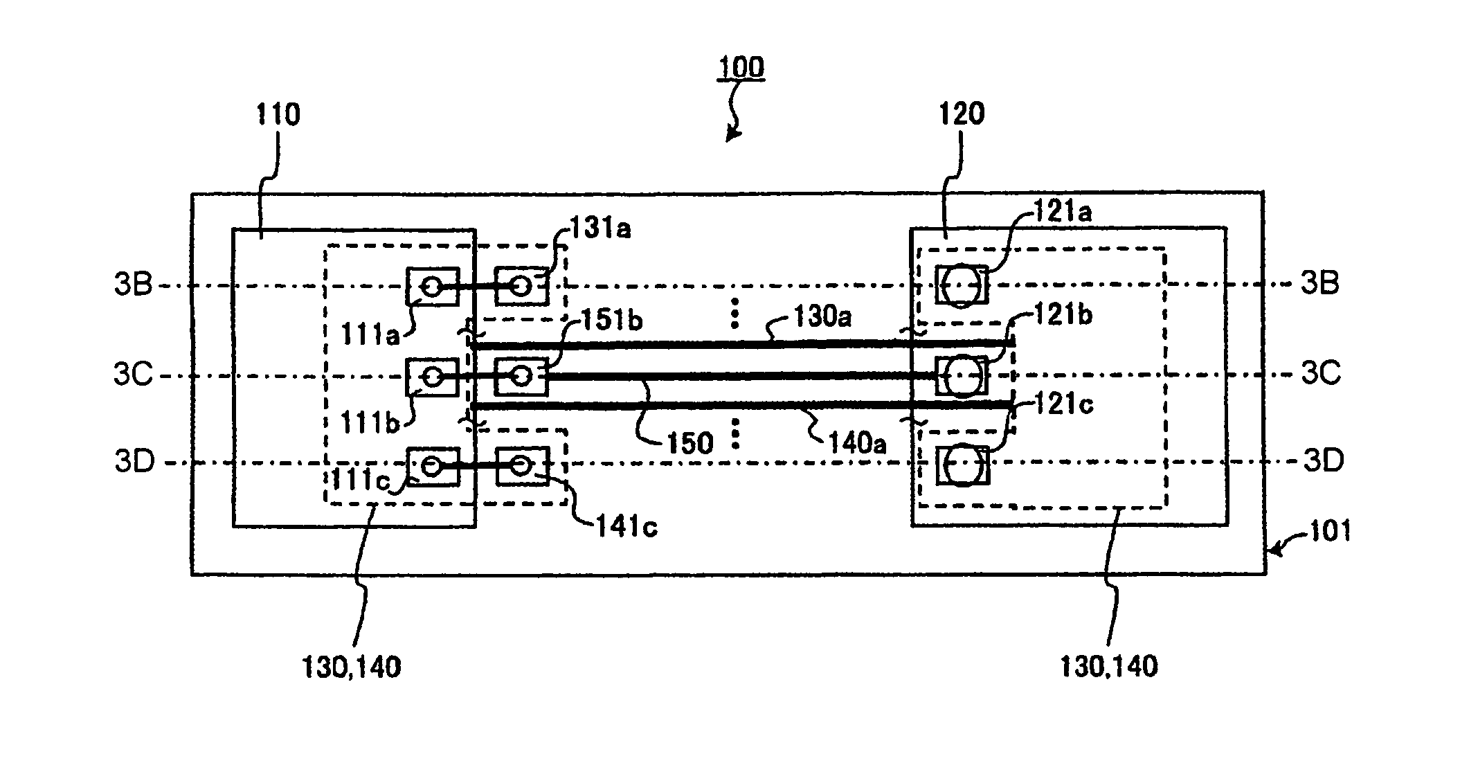
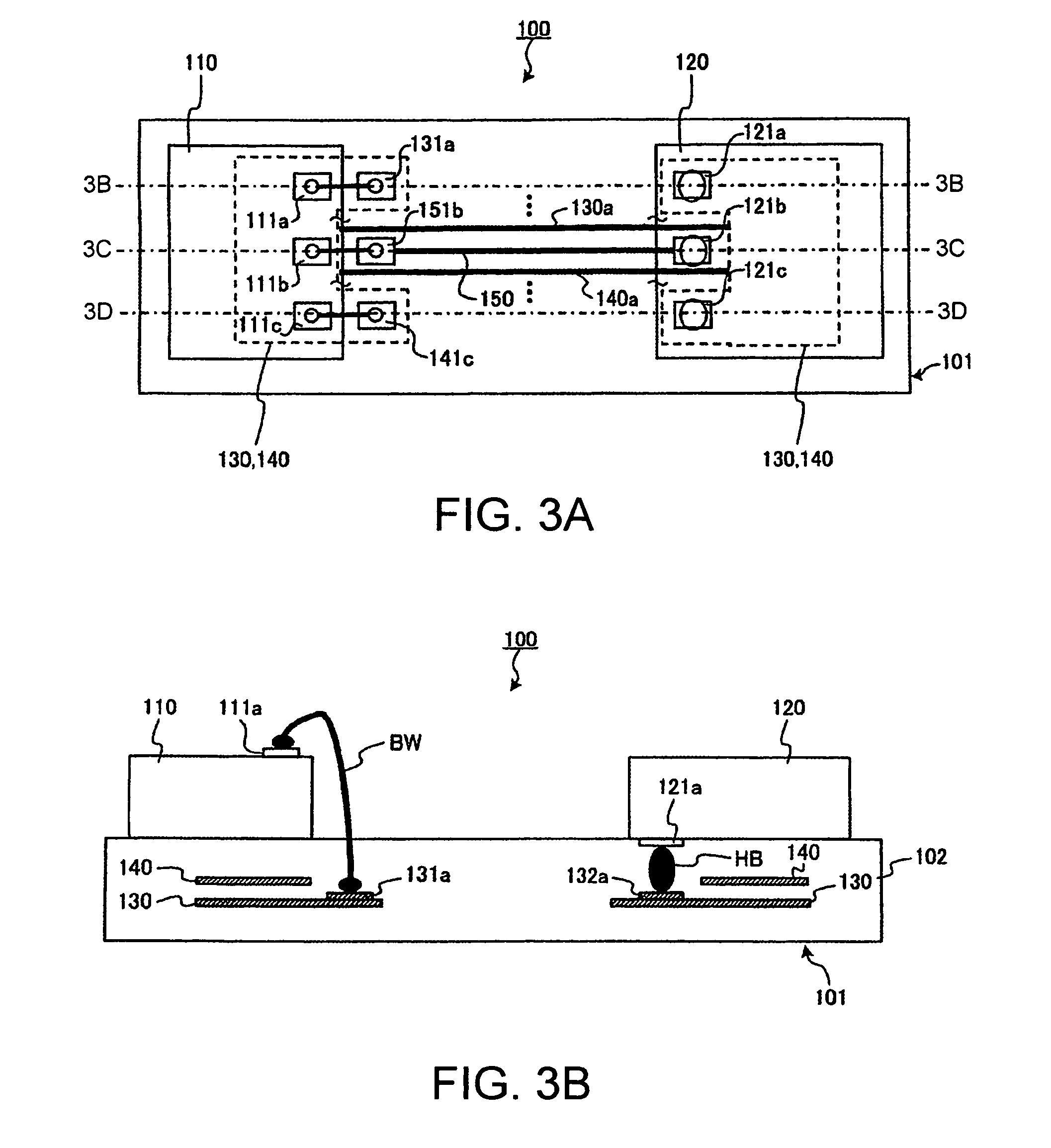
[0032]Referring to FIGS. 3A to 3E, a wiring structure of a substrate according to an embodiment of this invention will be described. The substrate in the embodiment is applicable to the case where various kinds of integrated circuits are mounted. For example, the integrated circuits may be a memory, a microprocessor, and a DSP (Digital Signal Processor).
[0033]Referring to FIGS. 3A to 3E, the wiring structure according to the embodiment is depicted by 100. A substrate 101 illustrated in the figures may be, for example, a semiconductor substrate of silicon of a double-layer structure. Not being limited to the semiconductor silicon substrate, this invention is applicable to an organic substrate or a ceramic substrate provided with an insulating film. IC chips 110 and 120 are mounted to the substrate 101. The IC chip 110 has a plurality of pads 111a, 111b, and 111c for wire bonding. The IC chip 120 has a plurality of pads 121a, 121b, and 121c for solder balls.
[0034]In the illustrated ex...
PUM
 Abstract
Description
Claims
Application Information