Semiconductor device

a technology of semiconductor devices and dielectric devices, which is applied in the direction of semiconductor devices, electrical devices, transistors, etc., can solve the problems of low read current, reduced switching speed of control gates and word gates, and difficulty in making thinners, so as to prevent potential barriers, prolong effective channel length, and suppress the effect of reading current lowering

Inactive Publication Date: 2012-01-31
NEC CORP
View PDF15 Cites 7 Cited by
  • Summary
  • Abstract
  • Description
  • Claims
  • Application Information

AI Technical Summary

Benefits of technology

[0017]According to this invention, a step is formed in a portion of a channel region at which the two gate electrodes are adjacent to each other, and electric fields from both of the gate electrodes are adapted to be applied to the step portion with the distance therebetween being at the minimum. Therefore, a potential barrier is prevented from being formed at the portion at which the two gate electrodes are adjacent to each other, and thus, lowering of the read current can be suppressed.
[0018]Further, the effective channel length is extended, and hence increase of a punch through current generated when the length of the gate electrodes is made smaller can be suppressed. Therefore, the on / off ratio of the read current can be made larger.

Problems solved by technology

However, from the 90 nm generation on, it becomes difficult to make thinner the insulating film in view of securing retention characteristics, and hence a trap type memory which uses as a charge storage layer a trap in an insulating film is attracting attention.
In order to increase the operation speed of the memory, it is necessary that the read current when the charge is erased be high, but, when the Twin MONOS type structure is used, there is a problem that the read current becomes low.
However, by making thin the insulating film between the word gate electrode and the control gates, a capacitance C between the word gate electrode and the control gates is increased, which lowers the switching speed of the control gates and the word gate.

Method used


Image

  • Semiconductor device
  • Semiconductor device
  • Semiconductor device

Examples


example 1

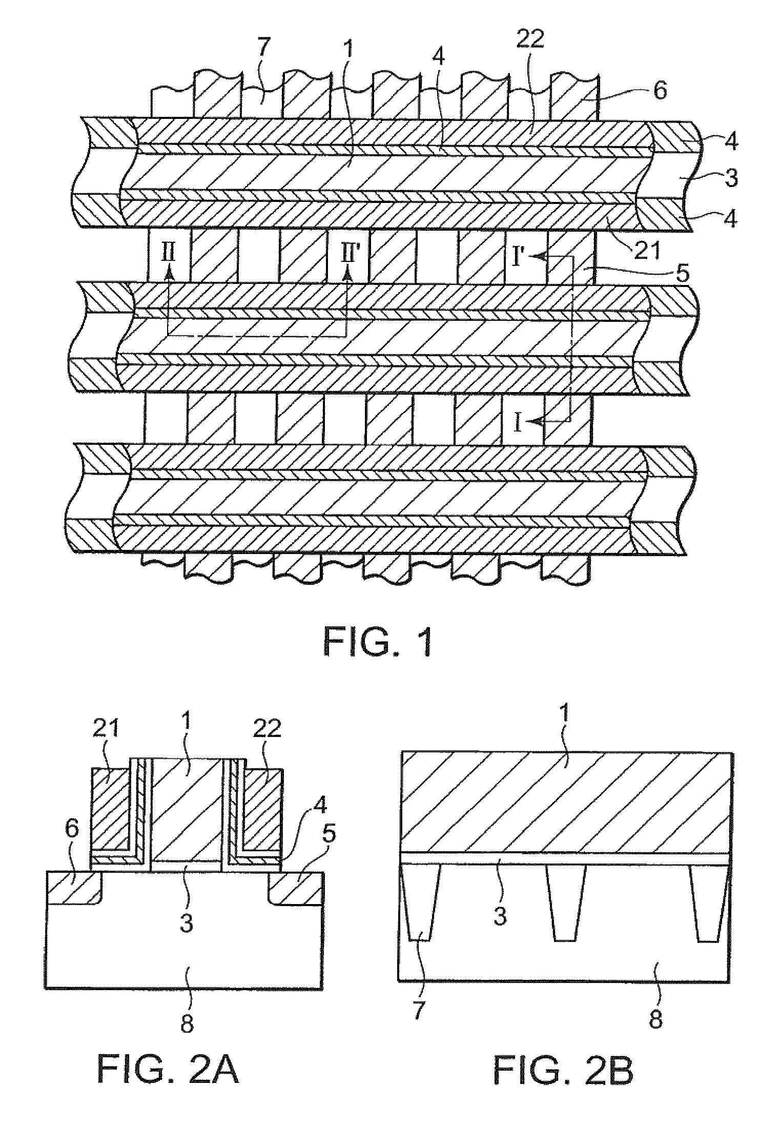
[0068]FIG. 7 is a plan view of a semiconductor storage device according to Example 1 of this invention, which is, here, a Twin MONOS storage device.

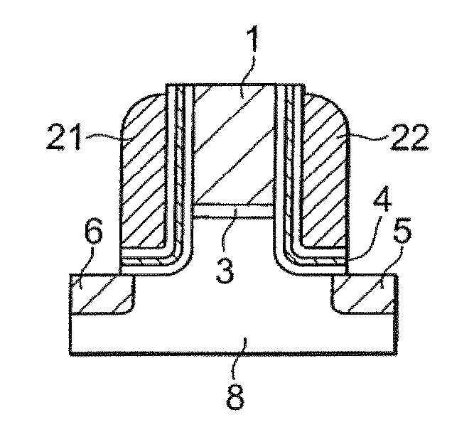
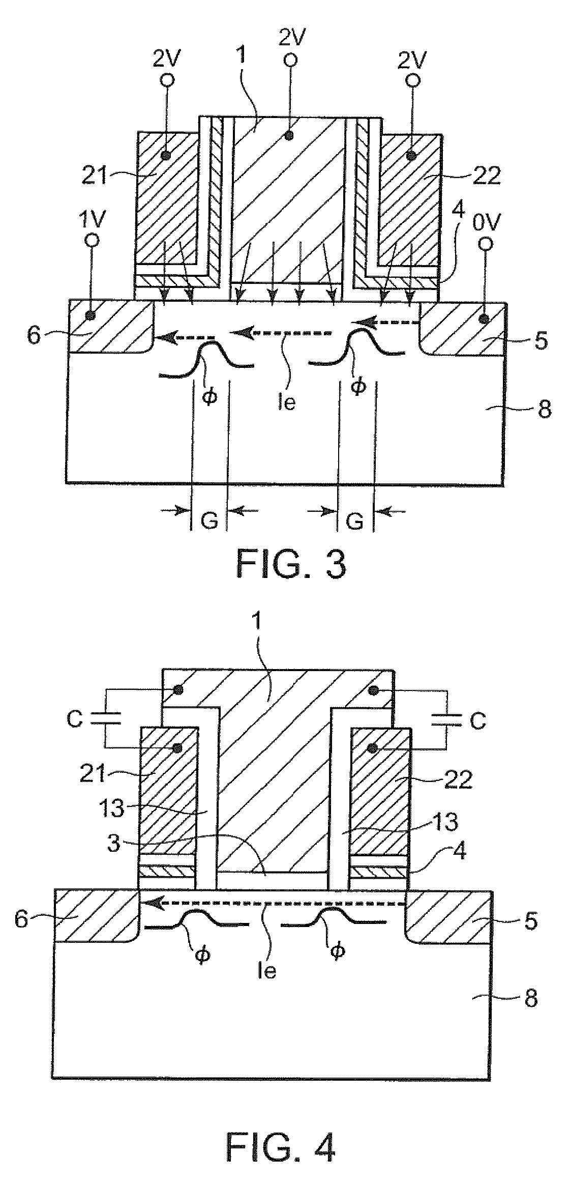
[0069]As illustrated in FIG. 7, in the storage device of this example, a device isolation region 7 is disposed in predetermined regions of a semiconductor substrate to define active regions including source-drain regions 5 and 6 and a channel region. The active regions are crossed by a plurality of word gate electrodes 1 and control gates 21 and 22. There is interposed a word gate insulating film 3 not including a charge storage layer between the word gate electrode 1 and the active region while there is interposed a trap insulating film 4 including a charge storage layer between the control gates 21 and 22 and the active region.

[0070]FIG. 8A and FIG. 8B are sectional views taken along the lines I-I′ and II-II′ of FIG. 7, respectively, which illustrate the storage device according to this example.

[0071]In the storage device of this examp...

example 2

[0082]FIG. 10 is a plan view of a semiconductor storage device according to Example 2 of this invention, which is, here, a Twin MONOS storage device.

[0083]As illustrated in FIG. 10, in the storage device of this example, a device isolation region 7 is disposed in predetermined regions of a semiconductor substrate to define active regions including source-drain regions 5 and 6 and a channel region. The active regions are crossed by a plurality of word gate electrodes 1 and control gates 21 and 22. There is interposed a word gate insulating film 3 not including a charge storage layer between the word gate electrode 1 and the active region while there is interposed a trap insulating film 4 including a charge storage layer between the control gates 21 and 22 and the active region.

[0084]FIG. 11A and FIG. 11B are sectional views taken along the lines I-I′ and II-II′ of FIG. 10, respectively.

[0085]In the semiconductor storage device of this example, as illustrated in FIG. 11A and FIG. 11B,...

example 3

[0097]FIG. 13 is a plan view of a semiconductor storage device according to Example 3 of this invention. As illustrated in FIG. 13, in the storage device of this example, a device isolation region 7 is disposed in predetermined regions of a semiconductor substrate to define active regions including source-drain regions 5 and 6 and a channel region. The active regions are crossed by a plurality of word gate electrodes 1 and control gates 2. There is interposed a word gate insulating film 3 not including a charge storage layer between the word gate electrode 1 and the active region while there is interposed a trap insulating film 4 including a charge storage layer between the control gate 2 and the active region. In this manner, a so-called split-gate semiconductor storage device was formed.

[0098]FIG. 14A and FIG. 14B are sectional views taken along the lines I-I′ and II-II′ of FIG. 13, respectively.

[0099]In Example 3, the active region is defined on a silicon substrate 8 by the devic...


PUM


Abstract

Provided is a semiconductor device including: source-drain regions formed on a silicon substrate with a channel forming region sandwiched therebetween; a word gate electrode formed on the channel forming region via a word gate insulating film not including a charge storage layer; a control gate formed on the silicon substrate on one side of the word gate electrode via a trap insulating film including a charge storage layer; and a control gate formed on the silicon substrate on the other side of the word gate electrode via a trap insulating film including a charge storage layer. A bottom of the word gate electrode is made to be higher than the control gate and a bottom of the control gate, and a level difference between the bottoms of the electrodes is made to be larger than a physical film thickness of the word gate insulating film.

Description

TECHNICAL FIELD[0001]This invention relates to a semiconductor device and a manufacturing technology thereof. More specifically, this invention relates to a semiconductor device including a rewritable nonvolatile semiconductor memory cell which is called a trap type.BACKGROUND ART[0002]With regard to flash memories up to the 0.13 μm generation, in order to miniaturize a flash memory, a dominant way of making smaller a flash memory is to make smaller a cell area using a Floating Gate (FG) type or to make thinner an insulating film. However, from the 90 nm generation on, it becomes difficult to make thinner the insulating film in view of securing retention characteristics, and hence a trap type memory which uses as a charge storage layer a trap in an insulating film is attracting attention.[0003]A Twin MONOS (Metal Oxide Nitride Oxide Semiconductor) type storage device is one type of trap type nonvolatile memories (see Japanese Patent Application Laid-Open No. 2005-142600 (Patent Docu...

Claims


Application Information

Patent Timeline
Patent Type & Authority Patents(United States)
IPC IPC(8): H01L29/792H01L29/04
CPCH01L21/28282H01L27/11565H01L27/11568H01L29/66833H01L29/7923H01L29/40117H10B43/30H10B43/10
Inventor TERAI, MASAYUKI
Owner NEC CORP
Why Eureka
Try Eureka