Method for doping non-planar transistors

a non-planar, doping technology, applied in the direction of basic electric elements, electrical equipment, semiconductor devices, etc., can solve the problems of poor contact, ion implantation damage the crystal structure of silicon, and inability to achieve doping techniques, etc., to achieve the effect of increasing the concentration of the doped conformal silicon glass layer

Inactive Publication Date: 2012-02-14
APPLIED MATERIALS INC
View PDF3 Cites 134 Cited by
  • Summary
  • Abstract
  • Description
  • Claims
  • Application Information

AI Technical Summary

Problems solved by technology

As device dimensions are reduced in order to achieve better performance and reduce the manufacturing costs, however, some doping techniques like ion implantation may not be feasible.
Ion implantation damages the crystal structure of the silicon due to high energy particle bombardment.
This becomes problematic especially in sub-micron dimensions where the device cannot tolerate crystal damage beyond a certain level, and using ion-implantation may result in poor contacts, increased junction leakage and increase in contact resistance.
Despite the desire of semiconductor manufacturers and others to adopt non-planar structures in both semiconductor devices and solar cells, there are challenges associated with doping the raised patterned silicon structures such as the drain, source and channel of FINFET 10 shown in FIG. 1.
The non-planar structures do not have the structural support that planar structures have, and thus their structural form may be damaged during doping, activation and etching.
Also, due to the small dimensions and shape of non-planar structures, thermal budget limitations may restrict the ability of device manufacturers to anneal damage induced during the doping process.

Method used


Image

  • Method for doping non-planar transistors
  • Method for doping non-planar transistors
  • Method for doping non-planar transistors

Examples


Embodiment Construction

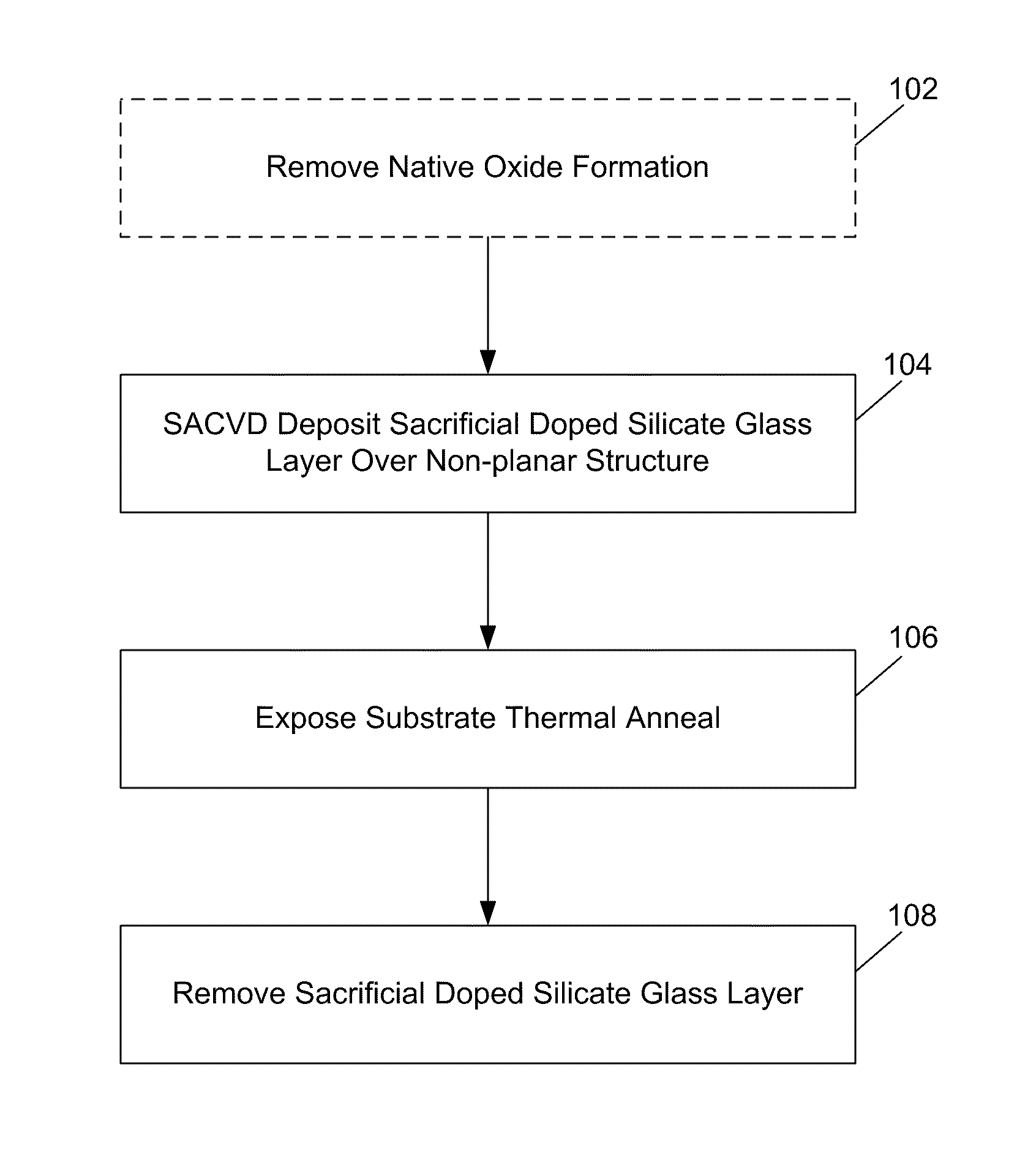
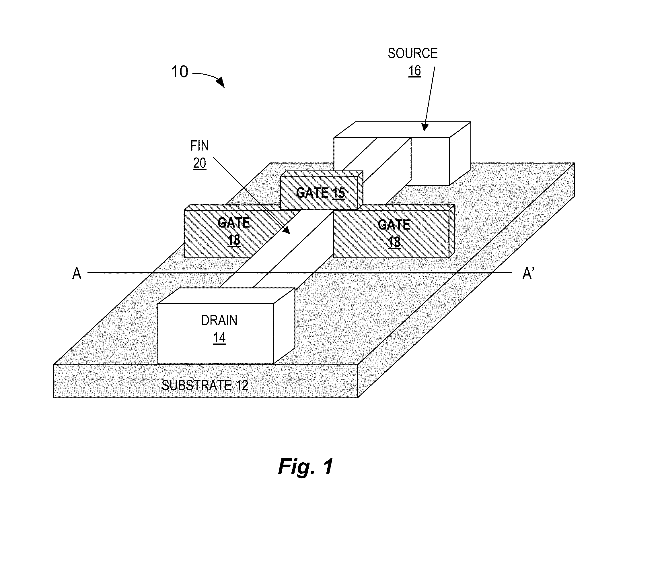
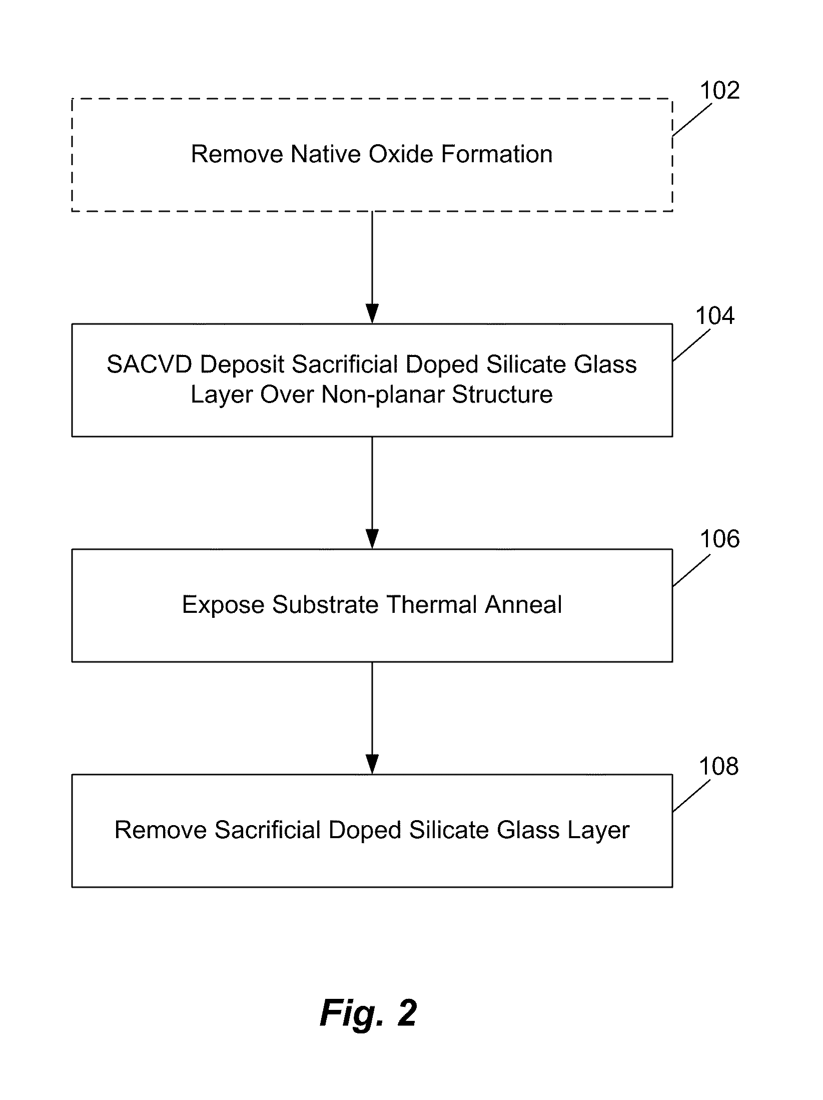
[0016]Doping non-planar structures require a degree of controllability that may be greater than what is needed for similarly dimensioned planar structures. For example, for multi-gate structures such as FINFET 10 shown in FIG. 1, uniform doping of the FIN structure helps to achieve Vt uniformity. Achieving this with ion implantation may require ion bombardment at large tilt angles that makes the process expensive and complex. The present inventors have come up with an improved dopant diffusion process that may advantageously be used to dope non-planar structures where doping uniformity and structural integrity is important. One embodiment of the method of the present invention uses a thermally driven SACVD deposition process to deposit a highly conformal sacrificial doped silicate glass layer over the non-planar structure. Deposition conditions are carefully controlled as described below to optimize dopant uniformity in a manner that is particularly well suited for non-planar struct...


PUM

PropertyMeasurementUnit
temperatureaaaaaaaaaa
pressureaaaaaaaaaa
temperatureaaaaaaaaaa

Abstract

Methods for doping a non-planar structure by forming a conformal doped silicon glass layer on the non-planar structure are disclosed. A substrate having the non-planar structure formed thereon is positioned in chemical vapor deposition process chamber to deposit a conformal SACVD layer of doped glass (e.g. BSG or PSG). The substrate is then exposed to RTP or laser anneal step to diffuse the dopant into the non-planar structure and the doped glass layer is then removed by etching.

Description

CROSS-REFERENCES TO RELATED APPLICATIONS[0001]This application claims the benefit of U.S. Provisional Patent Application No. 61 / 265,183, filed Nov. 30, 2009, and entitled “METHOD FOR DOPING NON-PLANAR TRANSISTORS,” which is incorporated herein by reference for all purposes.BACKGROUND OF THE INVENTION[0002]The present invention relates generally to doping non-planar structures such as those formed during the fabrication of some integrated circuits and photovoltaic cells. More particularly, the present invention relates to a method for providing a conformal dopant distribution on a non-planar silicon structure.[0003]A common technique used in fabrication of some semiconductor devices is to dope a silicon substrate with boron and / or phosphorus to adjust the electrical properties of the silicon. There are a variety of techniques used to dope planar structures formed on a silicon substrate including ion implantation, plasma doping and dopant diffusion. As device dimensions are reduced in...

Claims


Application Information

Patent Timeline
Patent Type & Authority Patents(United States)
IPC IPC(8): H01L21/00
CPCH01L21/2256H01L29/66803
Inventor MANDREKAR, TUSHAR V.VENKATARAMAN, SHANKARHUA, ZHONG QIANGHERNANDEZ, MANUEL A.
Owner APPLIED MATERIALS INC
Why Eureka
Try Eureka