Semiconductor device capable of providing identical strains to each channel region of the transistors

a technology of semiconductor devices and strains, applied in the direction of semiconductor devices, electrical devices, transistors, etc., can solve the problems of reducing the reliability of the semiconductor device, uneven strains of the transistors, and limited speed range of the transistor, so as to improve the reliability and performance of the device

Active Publication Date: 2012-02-14
UNITED MICROELECTRONICS CORP
View PDF4 Cites 4 Cited by
  • Summary
  • Abstract
  • Description
  • Claims
  • Application Information

AI Technical Summary

Benefits of technology

[0022]The semiconductor device of the present invention renders the channel region of each of the transistors with an identical strain to enhance the reliability and performance of the device.

Problems solved by technology

However, the speed range of the transistor is also limited by the moving speed of electrons and holes in silicon channels.
Thus, strains of the transistors are even more uneven.
Consequently, each of the transistors has different performance and reduces the reliability of the semiconductor device.

Method used


Image

  • Semiconductor device capable of providing identical strains to each channel region of the transistors
  • Semiconductor device capable of providing identical strains to each channel region of the transistors
  • Semiconductor device capable of providing identical strains to each channel region of the transistors

Examples


Embodiment Construction

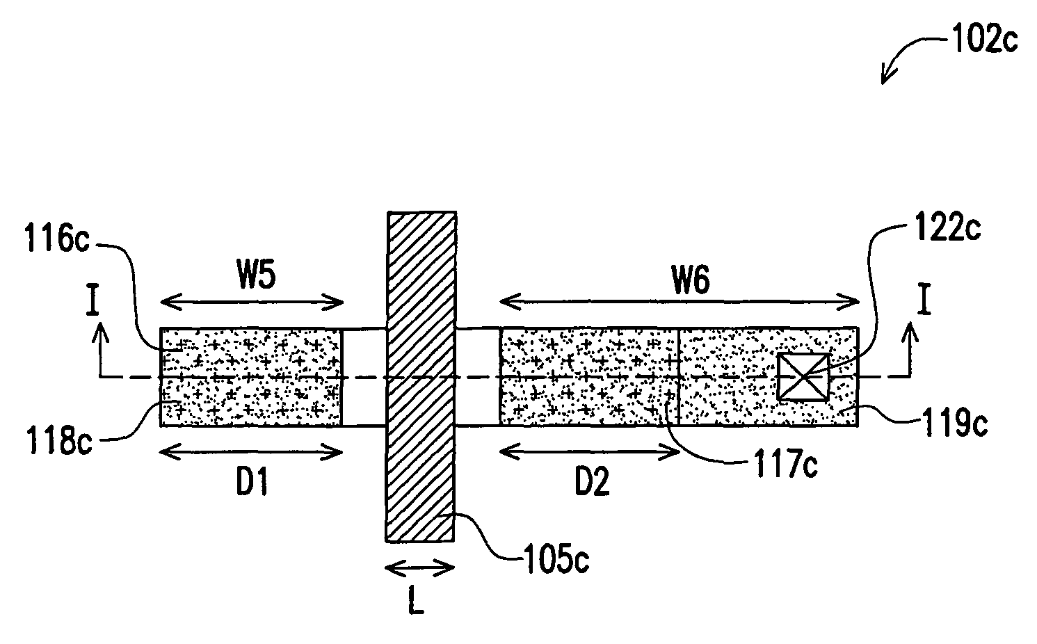
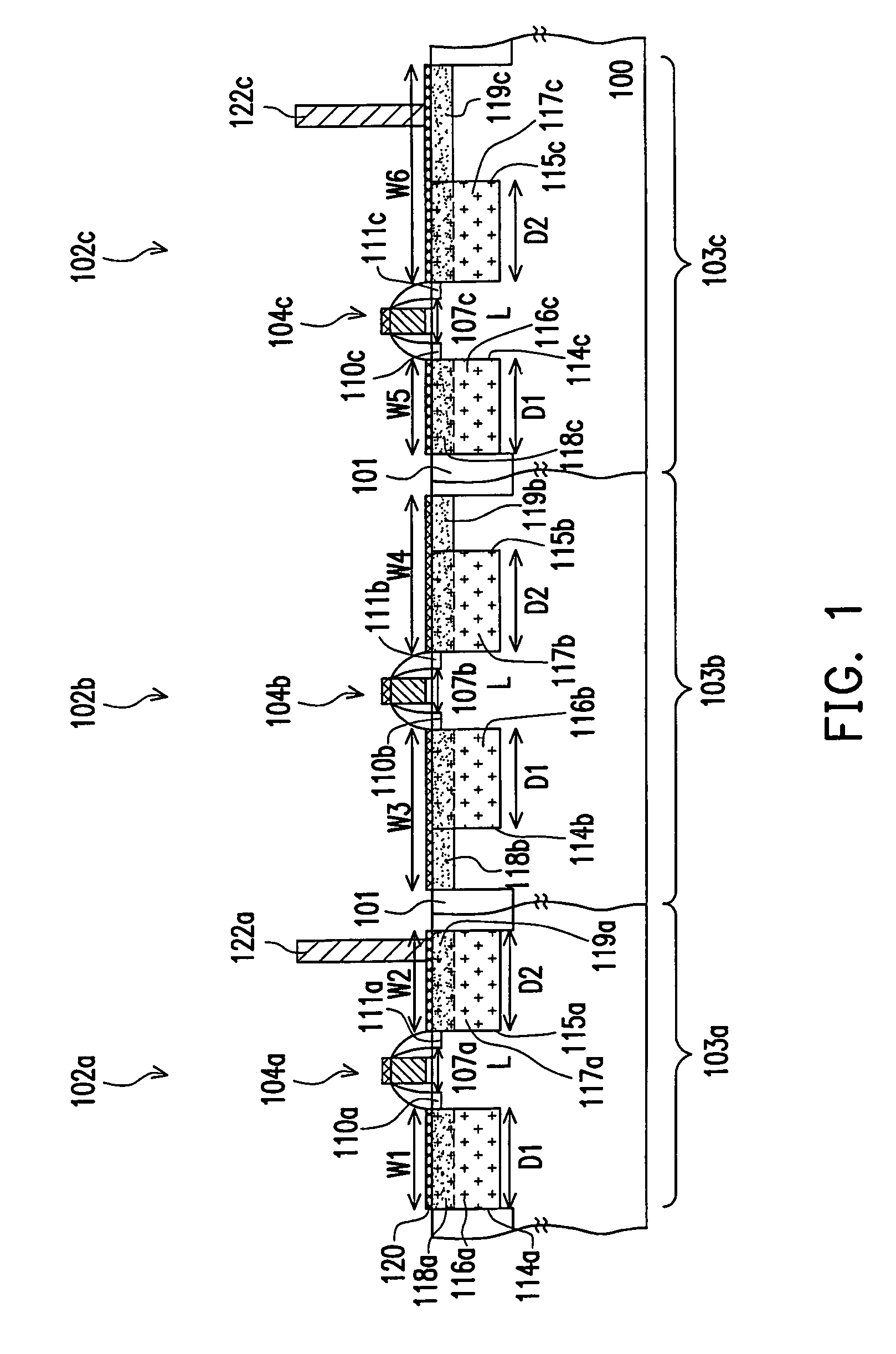
[0031]FIG. 1 is a schematic cross-sectional view illustrating a semiconductor device according to an embodiment of the present invention.

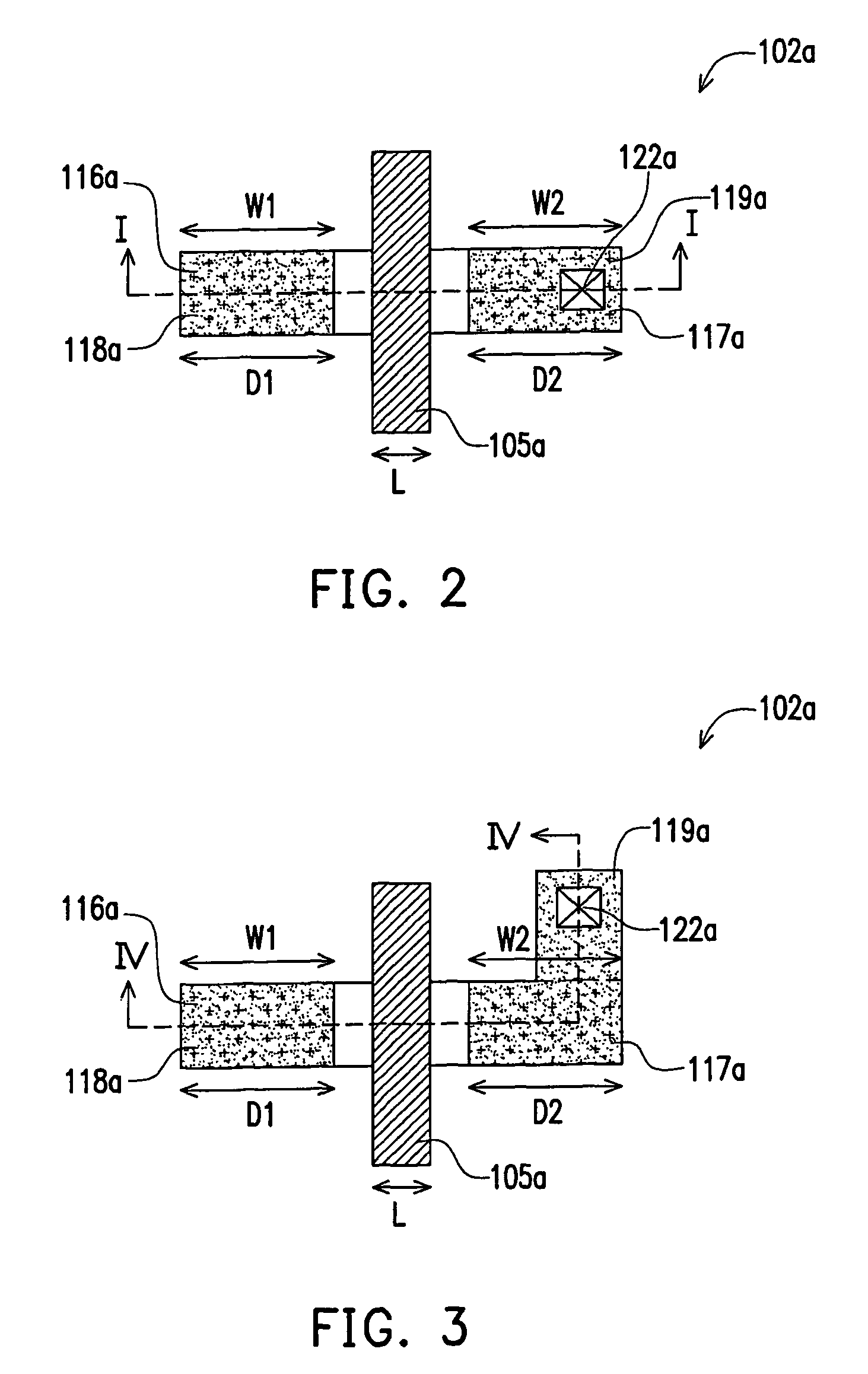
[0032]Referring to FIG. 1, the semiconductor device includes a plurality of transistors 102a, 102b and 102c having identical channel lengths and disposed on a substrate 100. The transistor 102a includes a gate structure 104a, a channel region 107a, source or drain extension regions 110a and 111a, strain layers 116a and 117a and source or drain regions 118a and 119a. The transistor 102b includes a gate structure 104b, a channel region 107b, source or drain extension regions 110b and 111b, strain layers 116b and 117b and source or drain regions 118b and 119b. The transistor 102c includes a gate structure 104c, a channel region 107c, source or drain extension regions 110c and 111c, strain layers 116c and 117c and source or drain regions 118c and 119c.

[0033]In the transistor 102a, the source or drain regions 118a and 119a are respectively disposed at ...


PUM


Abstract

A semiconductor device including transistors and strain layers is provided. Each transistor includes a source region and a drain region on a substrate and a gate structure on a channel region between the source region and the drain region. Lengths of the channel regions of these transistors are the same, but at least one source or drain region has a width along a channel length direction and the width is different from widths of other source or drain regions. The strain layers include first and second strain layers embedded separately at two sides of each gate structure in the substrate. A first width of each first strain layer along the channel length direction is the same, and a second width of each second strain layer along the channel length direction is the same.

Description

BACKGROUND OF THE INVENTION[0001]1. Field of the Invention[0002]The present invention relates to an integrated circuit structure and a method of fabricating the same, and more particularly, to a semiconductor device and a fabricating method thereof.[0003]2. Description of Related Art[0004]As development in electronic device technology such as communication devices advances, the operating speed of the transistor is getting faster and faster. However, the speed range of the transistor is also limited by the moving speed of electrons and holes in silicon channels.[0005]A method of increasing the operating speed of the transistor is to change the moving speed of electrons and holes in the channel through controlling the mechanical-stress in the channel. Taking a P-type channel metal oxide semiconductor (PMOS) as an example, in the prior art exists a technology of fabricating a source or drain region of the transistor mainly with a material such as SiGe epitaxy. Compared with the charact...

Claims


Application Information

Patent Timeline
Patent Type & Authority Patents(United States)
IPC IPC(8): H01L29/06
CPCH01L21/823412H01L21/823418H01L27/088H01L29/7848
Inventor YANG, CHIN-SHENG
Owner UNITED MICROELECTRONICS CORP
Why Eureka
Try Eureka