Electromagnetic shield structure of electronics housing

a technology of electronic housing and shield structure, which is applied in the direction of electrical apparatus casing/cabinet/drawer, casing/cabinet/drawer details, coupling device connections, etc., can solve the problems of increasing the cost of electronics housing, affecting the appearance, and reducing durability and operability, so as to achieve cost reduction

Active Publication Date: 2012-04-03
SANYO ELECTRIC CO LTD
View PDF37 Cites 39 Cited by
  • Summary
  • Abstract
  • Description
  • Claims
  • Application Information

AI Technical Summary

Benefits of technology

[0013]An object of the present invention is to provide an electromagnetic shield structure of an electronics housing by which, even in the case where there is a change in the type of the connection terminal to be attached, cost reduction can be achieved by minimizing the replacement of the mold used for manufacturing a housing component so as to accommodate the connection terminal.

Problems solved by technology

The electronics having a connection terminal connected to the outside is generally disposed within a housing because exposure of the electronics to the outside during use leads to a decrease in durability and operability.
The presence of the gap may result in adherence of dust and the like to the electronics, and also may impair the appearance.
Furthermore, there may also be a case where a baby's finger or the like is accidentally inserted into the gap.
Thus, even a slight change in the shape of the connection terminal requires at least three molds to be produced accordingly, which results in an increase in cost for the electronics housing.

Method used


Image

  • Electromagnetic shield structure of electronics housing
  • Electromagnetic shield structure of electronics housing
  • Electromagnetic shield structure of electronics housing

Examples


first embodiment

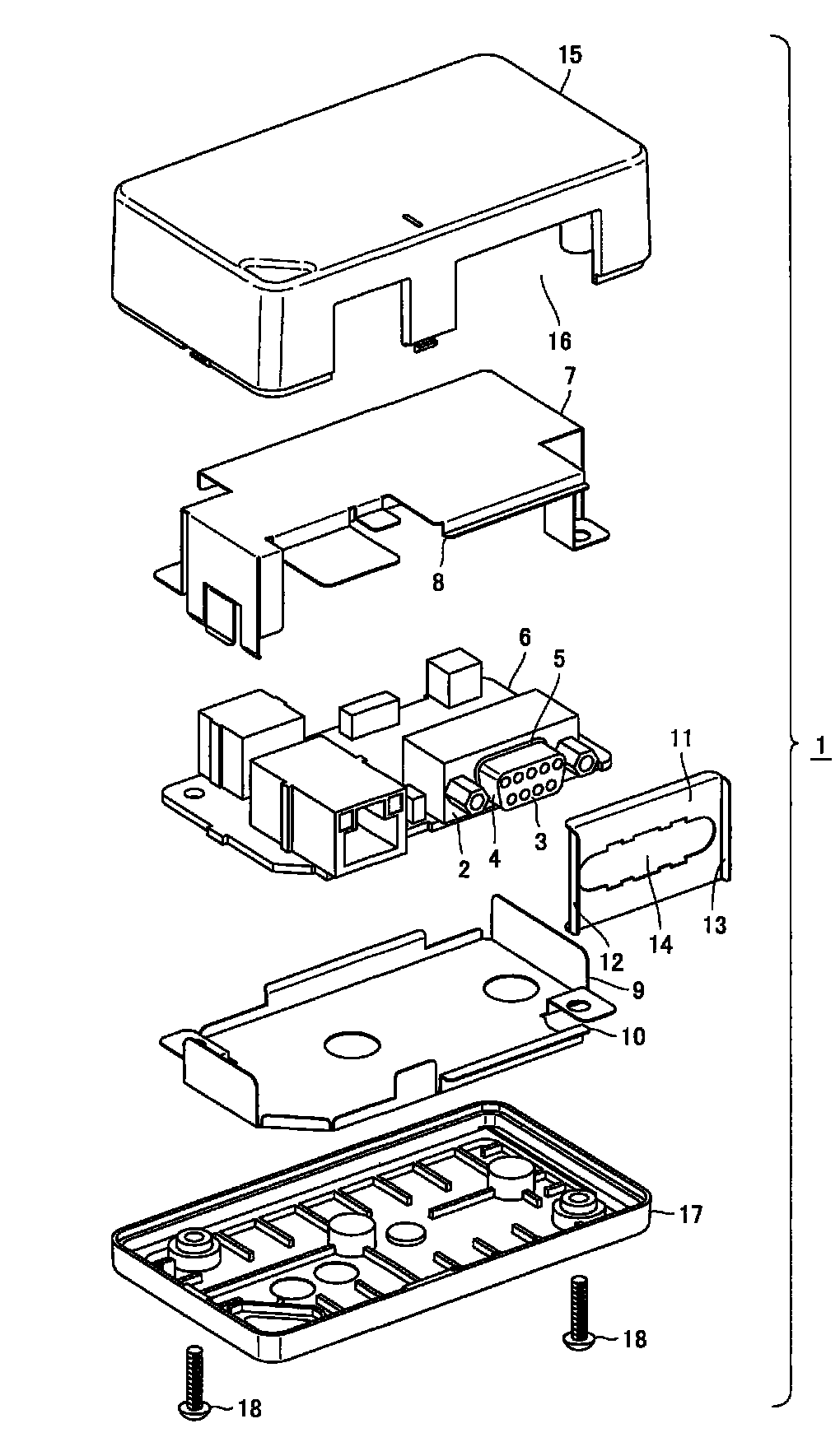
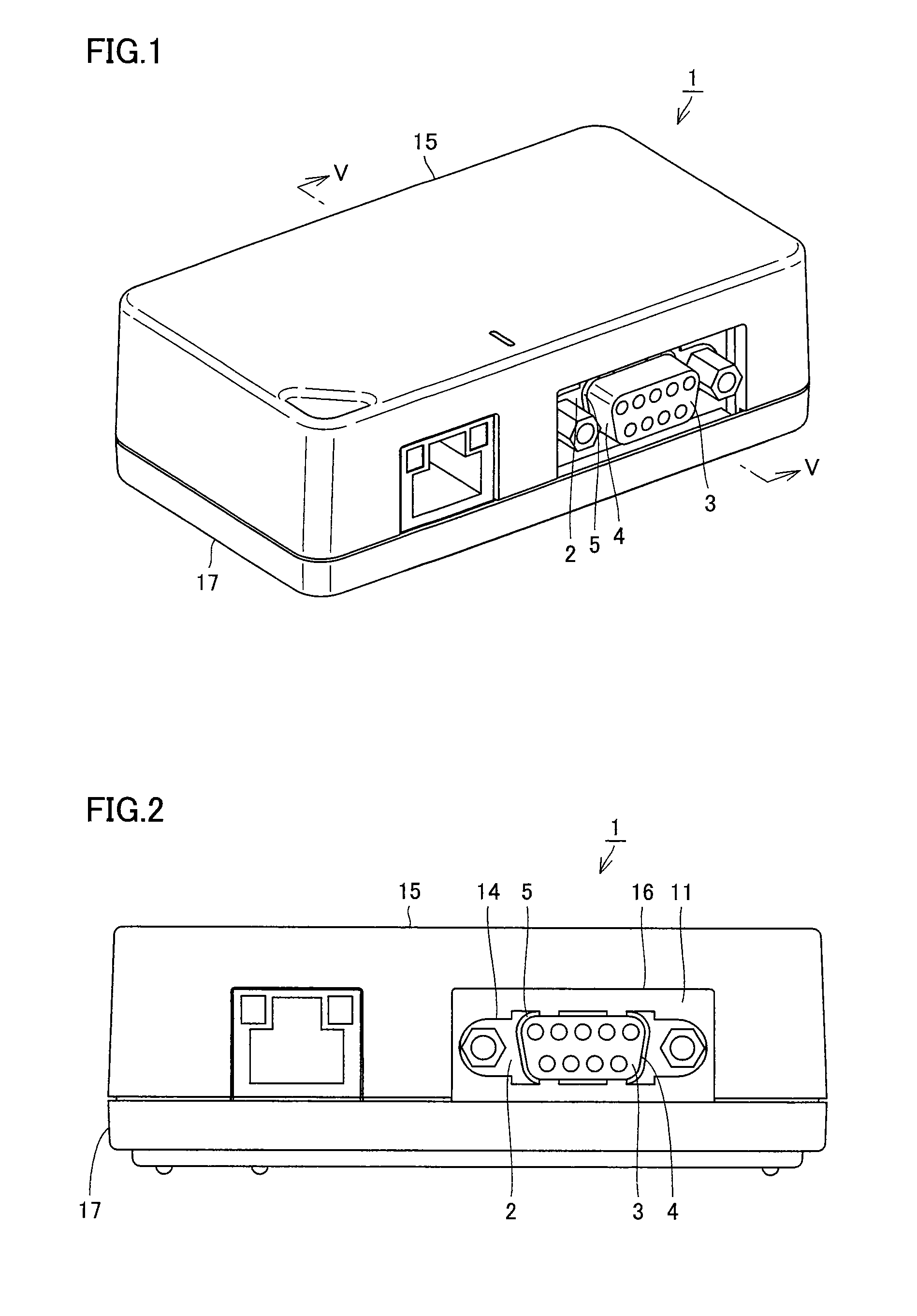
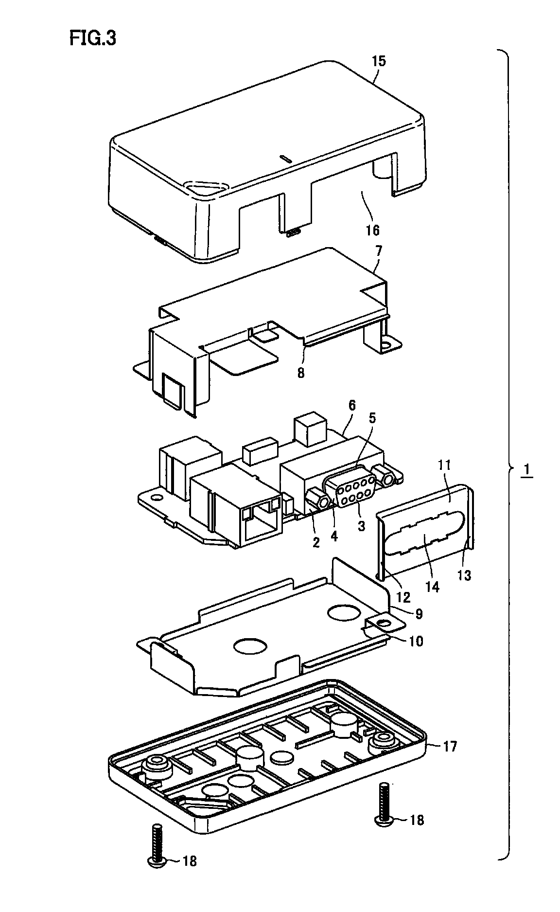
[0035]FIG. 1 is a perspective view of the outer appearance of an electronics housing according to the first embodiment of the present invention. FIG. 2 is a side view of the outer appearance of the electronics housing according to the present embodiment. FIG. 3 is an exploded perspective view of components of the electronics housing according to the present embodiment.

[0036]As shown in FIGS. 1 and 2, an electronics housing 1 according to the first embodiment of the present invention is formed as a housing having an exterior made of resin. The resin material may include thermosetting resin such as polycarbonate or polyacetal, or thermoplastic resin such as acrylonitrile-butadiene-styrene resin. Electronics housing 1 is equipped with a terminal 2 having a protrusion 3 for external connection. The housing includes an upper housing 15 and a lower housing 17. Upper housing 15 is provided on its front surface with an opening 16 that is formed at the position corresponding to protrusion 3 ...

second embodiment

[0051]FIG. 7 is an exploded perspective view of the electromagnetic shield structure of the electronics housing according to the second embodiment of the present invention. FIG. 8 is a perspective view showing the state where the substrate having the terminal connected thereto is surrounded by the electromagnetic shield. As shown in FIG. 7, the electromagnetic shield according to the second embodiment of the present invention includes a first shield member 20 disposed below substrate 6, a second shield member 19 disposed above substrate 6, and a third shield member 21 disposed at the position of substrate 6 where terminal 2 is connected and having an opening 26 accommodating protrusion 3 of terminal 2. Although the present embodiment shows the case where the electromagnetic shield consists of three members, the number of the members is not limited thereto.

[0052]On the peripheral region around opening 26 of third shield member 21, bent portions 22 and 23 facing the side surfaces, res...

third embodiment

[0057]In the electromagnetic shield structure of electronics housing 1 according to the third embodiment of the present invention, the inner edge of opening 14 of third shield member 11 and an outer periphery 4 of protrusion 3 of terminal 2 are pressed against each other to cause third shield member 11 to be biased toward the front surface side of the electromagnetic shield, such that first shield member 9 and second shield member 7 are brought into close contact with third shield member 11. Since the configuration other than the above is the same as that in the first or second embodiment, the description thereof will not be repeated.

[0058]For example, in the case where outer periphery 4 of protrusion 3 of terminal 2 is formed in the tapered shape in electronics housing 1 shown in FIG. 5, the size of opening 14 in third shield member 11 is set such that when third shield member 11 is inserted up to basal portion 5 of protrusion 3, outer periphery 4 at basal portion 5 of protrusion 3...


PUM


Abstract

An electromagnetic shield structure of an electronics housing includes a terminal having a protrusion for external connection; a substrate having the terminal disposed thereon and electrically connected to the terminal; a housing made of resin, enclosing the substrate and having an opening at a position corresponding to the protrusion of the terminal on a front surface side where the protrusion of the terminal is located; and an electromagnetic shield disposed so as to surround the substrate inside the housing, having an opening at the position corresponding to the protrusion of the terminal, and electromagnetically shielding the substrate. The electromagnetic shield has a bent portion formed on the front surface side for filling a gap between the terminal and the housing.

Description

BACKGROUND OF THE INVENTION[0001]1. Field of the Invention[0002]The present invention relates to an electromagnetic shield structure of an electronics housing for blocking an electromagnetic wave between the electronics and the outside thereof.[0003]2. Description of the Background Art[0004]The electronics having a connection terminal connected to the outside is generally disposed within a housing because exposure of the electronics to the outside during use leads to a decrease in durability and operability. Furthermore, the electronics are surrounded by an electromagnetic shield such that the electronics are electromagnetically shielded from the outside.[0005]There may be a case where the electromagnetic shield is provided with a function as an electromagnetic shield by forming a thin film having conductivity and electromagnetic-wave shielding properties on the inner surface of the housing, providing a protrusion having a shape of a flat spring on the periphery of a connection term...

Claims


Application Information

Patent Timeline
Patent Type & Authority Patents(United States)
IPC IPC(8): H05K9/00
CPCH05K9/002
Inventor NISHIHATA, YOSUKE
Owner SANYO ELECTRIC CO LTD
Why Eureka
Try Eureka