Early logic mapper during FPGA synthesis

a logic mapper and synthesis algorithm technology, applied in the field of programable logic devices, can solve the problems of inability of original equipment manufacturers (oems) to design and use asics, increase design costs, and complexity, and achieve the effects of improving power, area and frequency predictability, improving power, area and frequency, and reducing the performance of power and area

Active Publication Date: 2012-04-24
ALTERA CORP
View PDF17 Cites 1 Cited by
  • Summary
  • Abstract
  • Description
  • Claims
  • Application Information

AI Technical Summary

Problems solved by technology

Due to the advances of chip manufacturing technology, application specific integrated circuits (ASICs) designs have become incredibly complex.
This complexity not only adds to design costs, but also the duration of time needed to develop an application specific design.
As a result, it is often not feasible for original equipment manufacturers (OEMs) to design and use ASICs.
There is a problem with the synthesis modules of currently known programming software packages.
If the power, area and / or fmax parameters for a given design are not acceptable or less than ideal, however, there is very little that can be done to remedy the problem.
Generally speaking, the synthesis of the design at the Technology Mapping stage is too far along to implement any meaningful changes that would significantly impact or improve the power, area or fmax of the design.

Method used


Image

  • Early logic mapper during FPGA synthesis
  • Early logic mapper during FPGA synthesis
  • Early logic mapper during FPGA synthesis

Examples


Embodiment Construction

[0014]The present invention will now be described in detail with reference to a various embodiments thereof as illustrated in the accompanying drawings. In the following description, specific details are set forth in order to provide a thorough understanding of the present invention. It will be apparent, however, to one skilled in the art, that the present invention may be practiced without using some of the implementation details set forth herein. It should also be understood that well known operations have not been described in detail in order to not unnecessarily obscure the present invention.

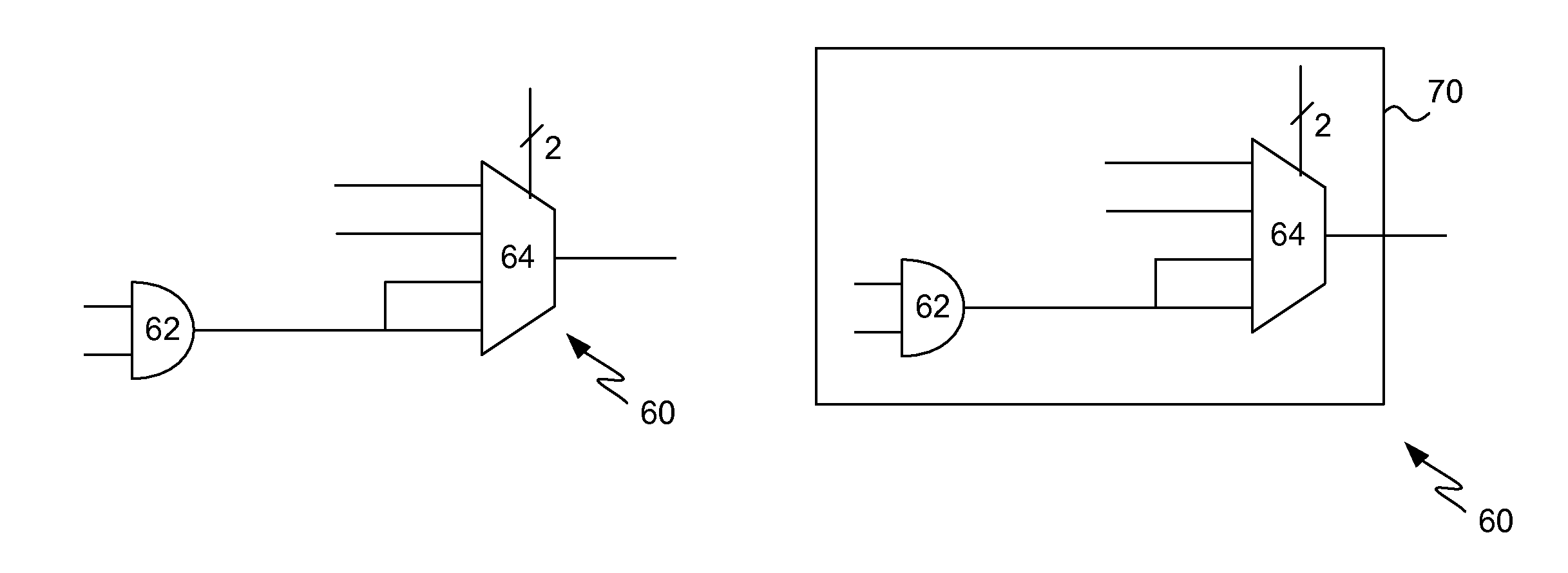
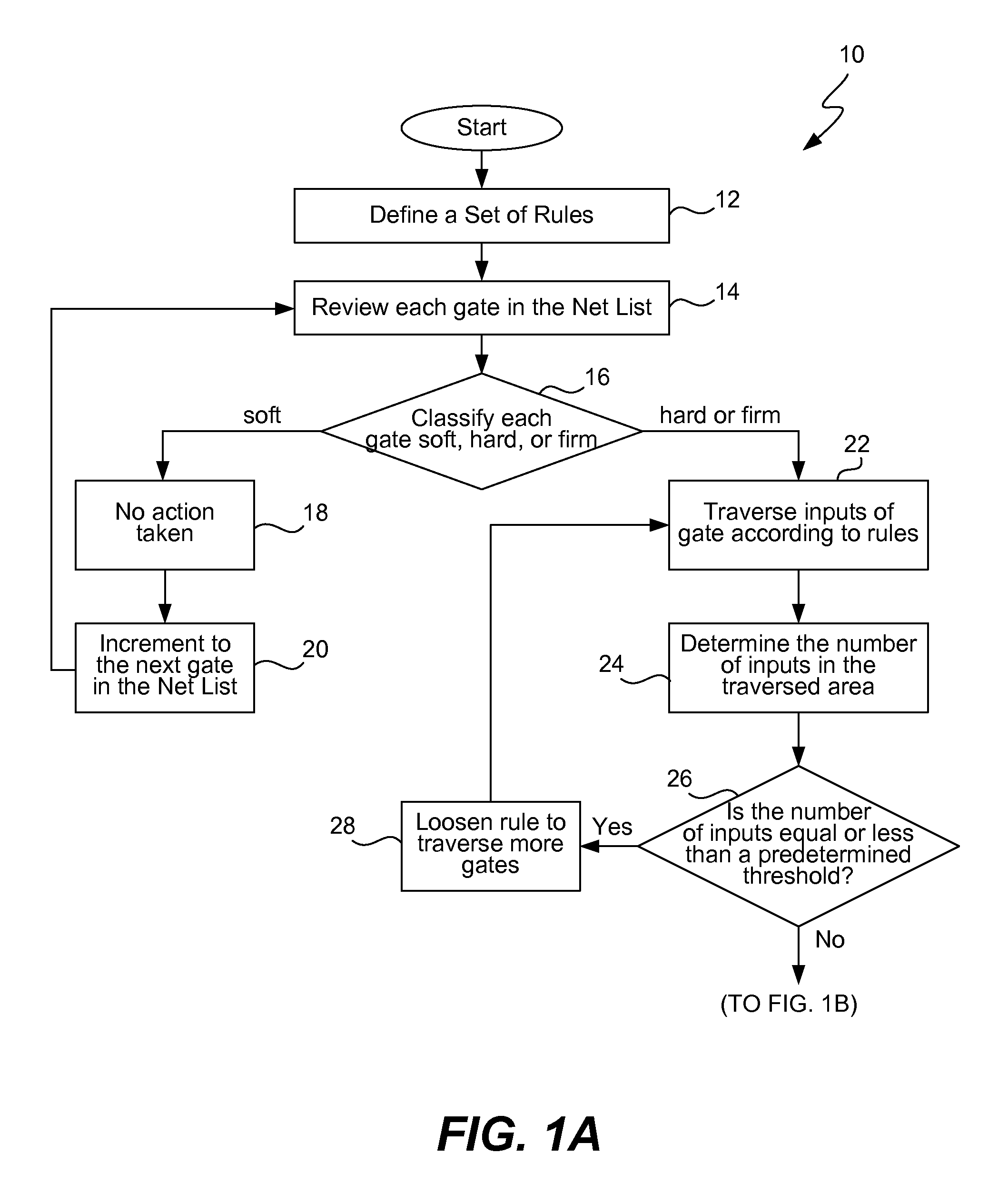
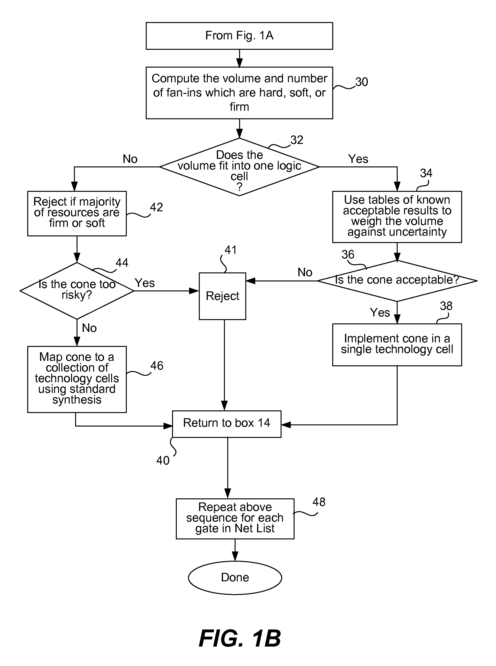
[0015]The present invention is related to a logic synthesis algorithm that improves the power, area and frequency predictability of a logic design early on during the High Level Synthesis, prior to Technology Mapping, without degrading the power, speed (Fmax) or area of the final design implementation. The High Level Synthesis algorithm involves a set of rules that identify situations where ...


PUM


Abstract

Programming software defining an algorithm that provides improved power, area and frequency predictability of a logic design early in the synthesis flow process, prior to Technology Mapping, without degrading the power, speed or area of the design implementation for PLDs. The method of the algorithm involves performing a high level synthesis of the logic design to generate a netlist, performing a multilevel synthesis on the netlist to generate a gate implementation of the netlist, and performing technology mapping on the gate implementation to map the gate implementation to actual resources on the target device. During the high level synthesis of the logic design into the netlist, technology mapping is performed on a selected portion of the logic design.

Description

CROSS-REFERENCED TO RELATED APPLICATIONS[0001]This application is a continuation of and claims the benefit of co-pending U.S. patent application Ser. No. 11 / 412,322 titled “Method For Early Logic Mapping During FPGA Synthesis”, filed on Apr. 26, 2006, which is incorporated herein by reference in its entirety for all purposes.FIELD OF THE INVENTION[0002]The present invention generally relates to programmable logic devices, and more particularly, to the programmable logic design software defining a synthesis algorithm that provides improved power, area and frequency predictability of a logic design early in the synthesis flow process, prior to technology mapping.BACKGROUND[0003]A Programmable Logic Device (PLD) is a semiconductor integrated circuit that contains fixed logic circuitry that can be programmed to perform a host of logic functions. In the semiconductor industry, PLDs are becoming increasingly popular for a number of reasons. Due to the advances of chip manufacturing techno...

Claims


Application Information

Patent Timeline
Patent Type & Authority Patents(United States)
IPC IPC(8): G06F17/50
CPCG06F17/5054G06F30/34
Inventor BAECKLER, GREGG WILLIAM
Owner ALTERA CORP
Why Eureka
Try Eureka