Semiconductor fabrication apparatuses to perform semiconductor etching and deposition processes and methods of forming semiconductor device using the same

a technology of semiconductor etching and deposition process and fabrication apparatus, which is applied in the direction of coating, chemical vapor deposition coating, electric discharge tube, etc., can solve the problems of increasing the production cost of the semiconductor device, and achieve the effect of shortening the moving line of the semiconductor fabrication process

Active Publication Date: 2012-06-12
SAMSUNG ELECTRONICS CO LTD
View PDF9 Cites 0 Cited by
  • Summary
  • Abstract
  • Description
  • Claims
  • Application Information

AI Technical Summary

Benefits of technology

[0010]The present general inventive concept also provides a method of forming a semiconductor device using a semiconductor fabrication apparatus to perform semiconductor etching and deposition processes at an edge of a semiconductor substrate to shorten a moving line of the semiconductor fabrication process.

Problems solved by technology

Thus, the method according to Japanese Patent Laid-open Publication No. 2002-334879 may prolong a processing time for forming the interconnection groove relating to the residues of the insulating layer, thereby increasing production cost of the semiconductor device.

Method used


Image

  • Semiconductor fabrication apparatuses to perform semiconductor etching and deposition processes and methods of forming semiconductor device using the same
  • Semiconductor fabrication apparatuses to perform semiconductor etching and deposition processes and methods of forming semiconductor device using the same
  • Semiconductor fabrication apparatuses to perform semiconductor etching and deposition processes and methods of forming semiconductor device using the same

Examples


Embodiment Construction

[0024]Reference will now be made in detail to embodiments of the present general inventive concept, examples of which are illustrated in the accompanying drawings, wherein like reference numerals refer to the like elements throughout. The embodiments are described below in order to explain the present general inventive concept by referring to the figures.

[0025]Semiconductor fabrication apparatus to perform semiconductor etching and deposition processes of the present general inventive concept will now be described in detail with reference to the accompanying drawings.

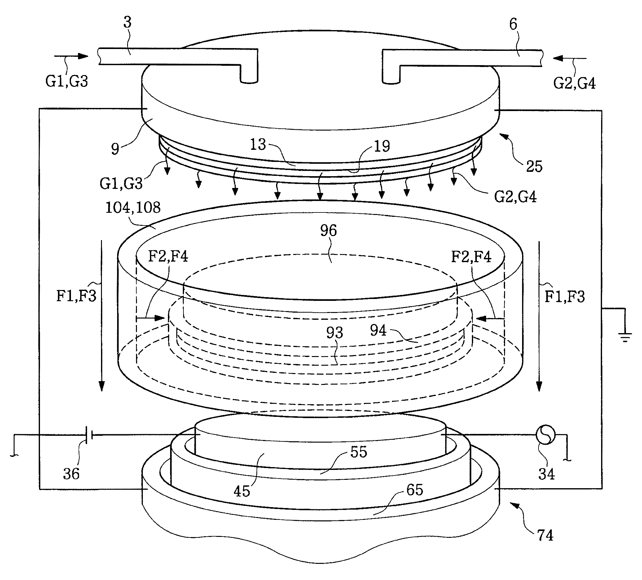
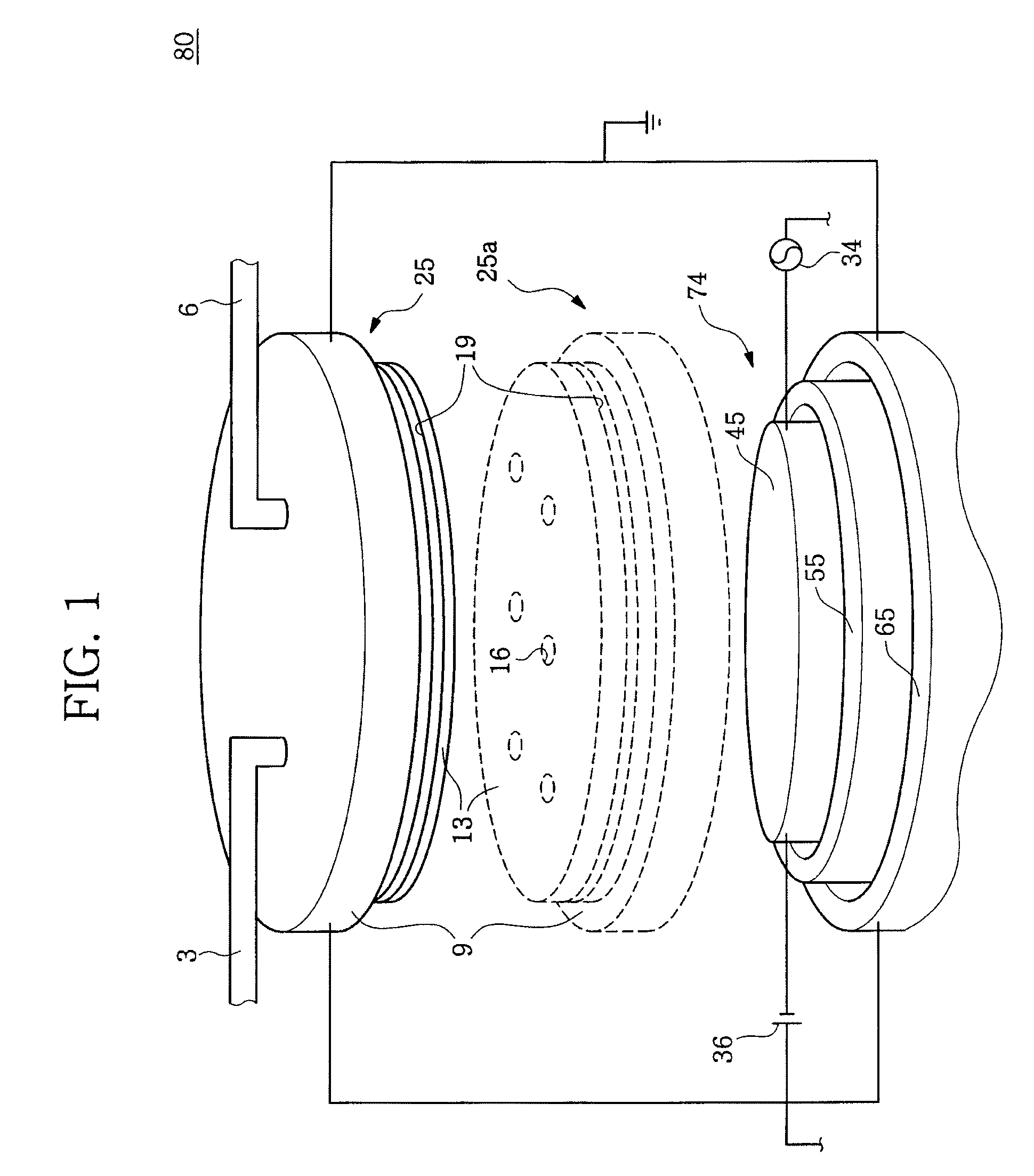
[0026]FIG. 1 is a schematic view illustrating a semiconductor fabrication apparatus according to an embodiment of the present general inventive concept.

[0027]Referring to FIG. 1, the semiconductor fabrication apparatus 80 according to the present embodiment includes a lower body 74. The lower body 74 has a lower electrode 65, an insulating housing 55 and a middle electrode 45. The middle electrode 45 has a same center a...


PUM

PropertyMeasurementUnit
diameteraaaaaaaaaa
electrical fieldaaaaaaaaaa
electrical potentialaaaaaaaaaa

Abstract

A semiconductor fabrication apparatus and a method of fabricating a semiconductor device using the same performs semiconductor etching and deposition processes at an edge of a semiconductor substrate after disposing the semiconductor substrate at a predetermined place in the semiconductor fabrication apparatus. The semiconductor fabrication apparatus has lower, middle and upper electrodes sequentially stacked. The semiconductor substrate is disposed on the middle electrode. Semiconductor etching and deposition processes are performed on the semiconductor substrate in the semiconductor fabrication apparatus. The semiconductor fabrication apparatus forms electrical fields along an edge of the middle electrode during performance of the semiconductor etching and deposition processes.

Description

CROSS-REFERENCE TO RELATED APPLICATIONS[0001]This patent application claims priority under 35 U.S.C. §119(a) from Korean Patent Application No. 10-2007-0019753, filed Feb. 27, 2007, the contents of which are hereby incorporated by reference in its entirety.BACKGROUND OF THE INVENTION[0002]1. Field of the Invention[0003]The present general inventive concept relates to semiconductor fabrication apparatuses and methods of forming a semiconductor device using the same, and more particularly, to semiconductor fabrication apparatuses to perform semiconductor etching and deposition processes and methods of forming the semiconductor device using the same.[0004]2. Description of the Related Art[0005]Typically, semiconductor devices are fabricated using a semiconductor substrate and a material layer. Here, the semiconductor devices may be configured to correspond to predetermined regions of the semiconductor substrate, respectively, thereby having electrical characteristics corresponding to t...

Claims


Application Information

Patent Timeline
Patent Type & Authority Patents(United States)
IPC IPC(8): H01L21/33
CPCH01J37/32009H01J37/32587H01L21/02057H01L21/02087H01L21/0209H01L21/205H01L21/3065
Inventor LEE, KYUNG-WOOKIM, JIN-SUNGYOON, JOO-BYOUNGLEE, YEONG-CHEOLPARK, SANG-JUNJEON, HEE-KYEONG
Owner SAMSUNG ELECTRONICS CO LTD
Why Eureka
Try Eureka