Electrode component and method for fabricating the same

a technology of electrode layer and electrode layer, which is applied in the direction of resistive material coating, fixed capacitor details, metal/alloy conductors, etc., can solve the problems of high production cost, unsatisfactory bonding strength between silver electrode layer and ceramic substrate, and high production cost of precious silver material, so as to reduce the risk of separable electrode interface, reduce production cost, and shorten the fabrication process of electrode layer

Active Publication Date: 2016-09-20
THINKING ELECTRONICS INDAL
View PDF13 Cites 0 Cited by
  • Summary
  • Abstract
  • Description
  • Claims
  • Application Information

AI Technical Summary

Benefits of technology

[0013]An objective of the present invention is to provide an electrode component and a method for fabricating the same allowing electrode layers of the electrode component to be formed of two or more metal materials sequentially stacked and the electrode layers and a ceramic substrate to be tightly bonded with good solderability.
[0027]Under the premise of original electrical characteristics of products, the benefits of the present invention includes lower production cost, no environment pollution arising from evaporation and thermal dissolution of organic solvent used in silk-screen printed conventional silver electrode, and reduced risk of separable electrode interface at high-voltage discharge because of bonding strength issue between different metal materials. Accordingly, the fabrication process of electrode layer is shortened while maintaining bonding strength between the electrode and the ceramic substrate and the solderability of the metal pins.

Problems solved by technology

However, conventional silk-screen printing process has the following drawbacks and deficiencies.
1. Lots of toxic substances contained in the organic silver paste cause serious environmental pollution.
2. High production cost arises from the use of a great deal of precious silver material.
1. Low bonding strength due to the silver-ceramic incompatibility. The bonding strength is increased mainly through the glassy substance in the organic silver paste diffused to the grain boundaries of ceramic, such that the bonding strength between the silver electrode layer and the ceramic substrate is not satisfactory.
2. High-resistance ohmic contact.
3. Poor corrosion resistance of the silver electrode layer against lead-free solder. As the solid solubility of silver and tin is relatively high, solder can easily etch a silver layer at a high temperature. Nowadays, owing to the concern of environmental protection, products are manufactured using the lead-free soldering technique. To avoid pseudo soldering and melting silver, the 3Ag solder indicative of a Sn—Ag—Cu solder alloy with a higher silver content at a weight percentage of silver 3% is used for soldering and thus becomes a cost-down barrier of products. Meanwhile, because of the high mutual solubility of tin and silver in a lead-free solder, after products are powered on and operated for a long time, the silver electrode layer can be easily etched by the solder, such that the electrode has a reduced adhesion force and even becomes detached. Therefore, once the electrode becomes detached, transportation equipment, such as vehicles, using such type of varistor could be in a dangerous situation.
To lower production cost of the varistors, as disclosed in China Patent Application No. 201310177249.5, entitled “Base metal combination electrode of electronic ceramic element and preparation method therefor”, the drawback of the electrode of the varistor fabricated using a technique of hot-spraying multiple layers of base metal resides in that upon a high-voltage discharge current gives rise to high heat at metal electrode interfaces and the metal electrode interfaces could be easily separable, hindering durability and reliability of products.

Method used


Image

  • Electrode component and method for fabricating the same
  • Electrode component and method for fabricating the same
  • Electrode component and method for fabricating the same

Examples


Embodiment Construction

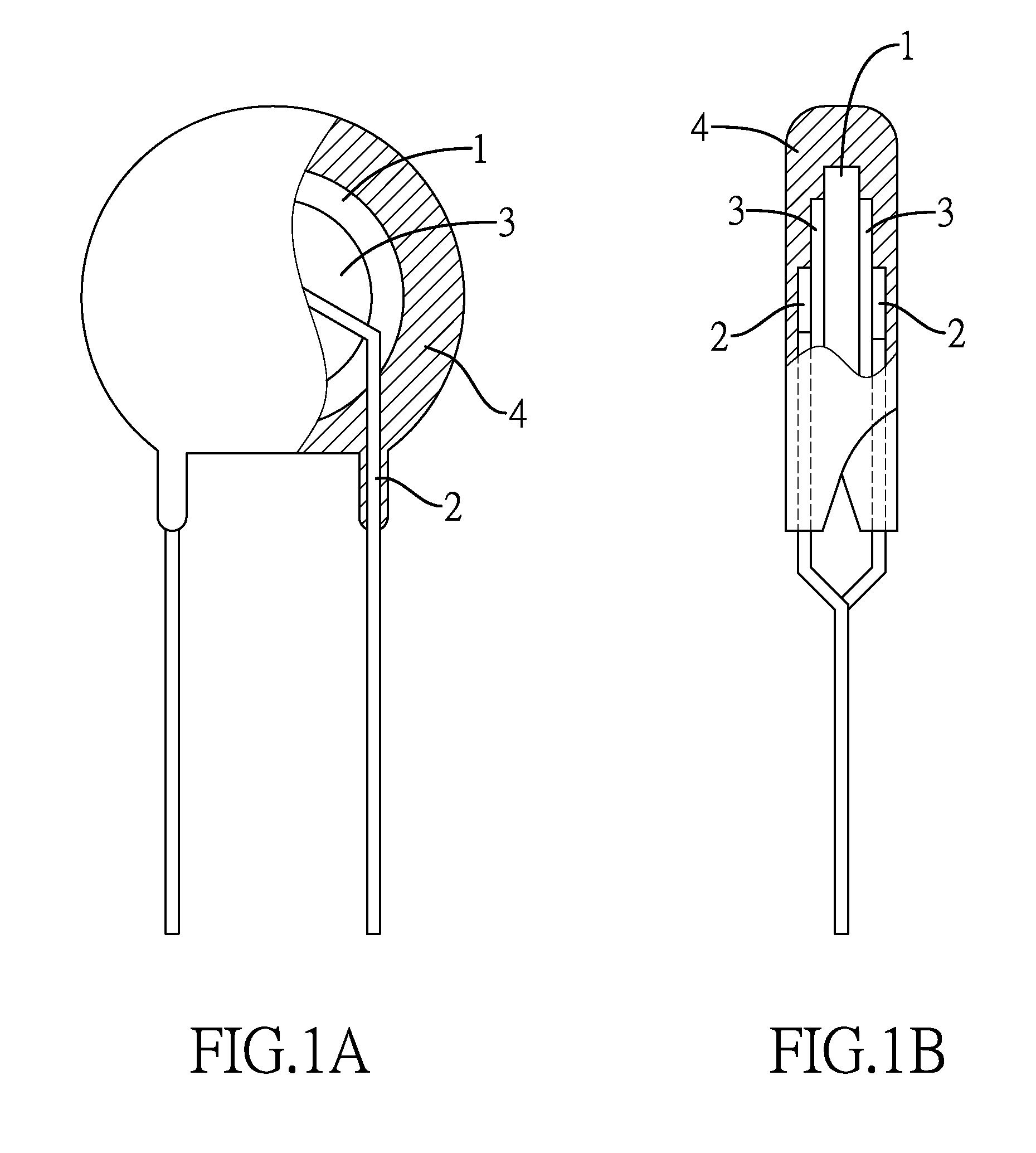
[0035]With reference to FIGS. 1A and 1B, an electrode component in accordance with the present invention includes a ceramic substrate 1, two electrode layers 3, two pins 2 and an insulating layer 4.

[0036]The two electrode layers 3 are respectively formed on two opposite surfaces of the ceramic substrate 1. The two pins 2 are respectively connected to the electrode layers 3. The insulating layer 4 encloses the ceramic substrate 1, the electrode layers 3 and a portion of each pin 2.

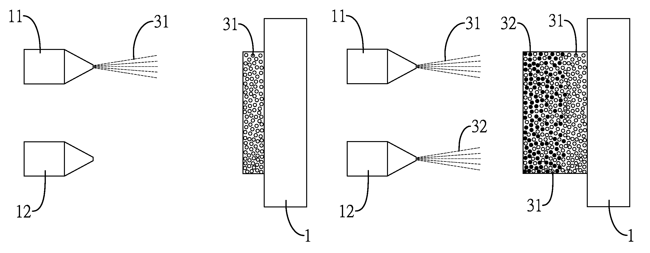
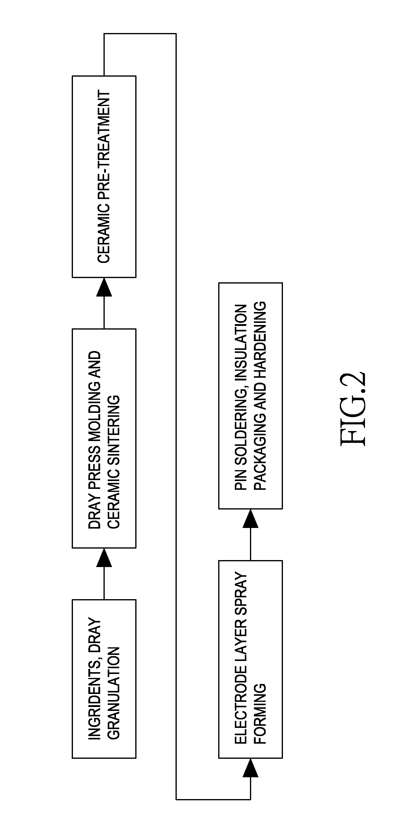
[0037]With reference to FIG. 2, a method for fabricating an electrode component in accordance with the present invention is shown. Given the electrode component as a varistor, the method includes steps of spray granulation, dry press molding, ceramic sintering and ceramic pre-treatment, which are known as conventional techniques and are not repeated here. After the ceramic substrate 1 is pre-treated, a process of spray-forming the electrode layers 3 and subsequent steps for pin soldering, insulation packagi...


PUM

PropertyMeasurementUnit
thicknessaaaaaaaaaa
timeaaaaaaaaaa
temperatureaaaaaaaaaa

Abstract

An electrode component includes a ceramic substrate, two electrode layers formed on two opposite surfaces of the ceramic substrate, two pins respectively connected to the two electrode layers, and an insulating layer enclosing the ceramic substrate, the electrode layers and a portion of each pin. Each electrode layer is formed of two or more base metal materials or alloys thereof, and the concentrations of the base metal materials progressively vary across the electrode layer. Accordingly, the production cost is lowered, environmental pollution caused by evaporation and thermal dissolution of organic solvent can be prevented, risk of separable electrode interface at high-voltage discharge is mitigated, and the fabrication process of the electrode layer is shortened while maintaining bonding strength between the electrode layers and the ceramic substrate and solderability between the electrode layers and the pins.

Description

BACKGROUND OF THE INVENTION[0001]1. Field of the Invention[0002]The present invention relates to an electrode of an electrode component, and more particularly, to an electrode component with an electrode layer formed of two or more different metal materials and a method for fabricating the same.[0003]2. Description of the Related Art[0004]A varistor is an electronic component mainly formed by zinc oxide powder and mixed with bismuth oxide, antimony oxide, manganese oxide and the like diffused to grain boundaries of zinc oxide. After the mixture is molded by a dry press process, organic binder is removed from the mixture and a ceramic resistor with nonlinear characteristics is generated from the molded mixture using a high-temperature sintering process.[0005]The conductive electrode layer of a conventional varistor is usually formed by the silk-screen printing technique. During fabrication of the electrode layer, a ceramic chip with organic silver paste having a weight percent range ...

Claims


Application Information

Patent Timeline
Patent Type & Authority Patents(United States)
IPC IPC(8): H01C1/142H01C7/102H01G4/232H01C17/06H01C7/12H01G4/252H01B1/02H01C17/28H01C1/014H01C1/144
CPCH01C1/142H01B1/02H01C7/102H01C7/12H01C17/06H01C17/281H01C17/283H01G4/232H01G4/252H01C1/014H01C1/144
Inventor HUANG, JEN-HENG
Owner THINKING ELECTRONICS INDAL
Why Eureka
Try Eureka