Methods and devices for manufacturing cantilever leads in a semiconductor package

a technology of semiconductor packaging and cantilever leads, which is applied in the direction of semiconductor devices, semiconductor/solid-state device details, electrical apparatus, etc., can solve the problems of inability to use during die mounting and/or wire bonding processes, inability to manufacture custom heater block inserts, and high cost of purchase and maintenance, so as to achieve flexible and robust, the effect of expensive purchase and maintenan

Active Publication Date: 2012-07-10
TEXAS INSTR INC
View PDF4 Cites 2 Cited by
  • Summary
  • Abstract
  • Description
  • Claims
  • Application Information

AI Technical Summary

Benefits of technology

[0006]Applicant has recognized that there is a need for methods and devices for supporting cantilever leads during the assembly of semiconductor packages that are more flexible and robust than existing practices such as custom-built heater block inserts or leads each etched to have a standoff. Applicant has also recognized that custom-built heater block inserts, in addition to being expensive to purchase and maintain, cannot be used during die mount and / or wire bonding processes if a layer of adhesive film has been applied to a leadframe's bottom surface, for example, by the leadframe manufacturer. Applicant has further recognized that cantilever leads etched to have standoffs leave exposed metal features at the bottom surface of a finished semiconductor package, which renders the finished semiconductor package susceptible to short circuits caused by stray solder or PCB routing metal. Therefore, it is a technical advantage to assemble semiconductor packages without the need for expensive custom-built heater block inserts or leads etched to have standoffs.
[0009]Applicant then noted that leadframes are often supplied with a layer of tape, which is typically an unpatterned rectangular piece of plastic that is peeled off the leadframe subsequent to the molding process. Applicant considered this layer of tape as a good canvas on which the non-conductive material can be painted or applied to form one or more supports for supporting the cantilever leads. Correctly shaped, the non-conductive supports would remain in the molded semiconductor package. While considering the shapes of the non-conductive supports, Applicant realized that the footprint of the supports was no longer a restrictive factor with respect to PCB routing options because they were non-conductive. Therefore, the supports could fill in below the full lead or extend from lead to lead and support one or more cantilever leads against vertical motion and other undesired movement during the die mounting, wire bonding, and molding processes.
[0012]Using non-conductive supports to support cantilever leads eliminates the need for expensive custom-built heater block inserts or an inventory thereof for various leadframe designs, which results in greater processing flexibility, better cantilever lead support during various stages of package assembly, and cost savings. Using non-conductive supports also enhances the robustness and yield of integrated circuits and devices that incorporate the semiconductor package by minimizing exposed metal features thereon, which reduces features that can be short-circuited and allows greater PCB routing options under the semiconductor package.

Problems solved by technology

Applicant has also recognized that custom-built heater block inserts, in addition to being expensive to purchase and maintain, cannot be used during die mount and / or wire bonding processes if a layer of adhesive film has been applied to a leadframe's bottom surface, for example, by the leadframe manufacturer.
Applicant has further recognized that cantilever leads etched to have standoffs leave exposed metal features at the bottom surface of a finished semiconductor package, which renders the finished semiconductor package susceptible to short circuits caused by stray solder or PCB routing metal.
However, PCB routing requirements for certain applications, such as battery products, precluded the use of exposed thermal pad because routing space on the PCB was at a premium.
The full thickness metal standoffs, however, resulted in exposed metal features in the assembled semiconductor packages.
However, such a process would involve a complex pattern that needs to be photo-imaged, which would be challenging to accomplish on a fully etched leadframe.

Method used


Image

  • Methods and devices for manufacturing cantilever leads in a semiconductor package
  • Methods and devices for manufacturing cantilever leads in a semiconductor package
  • Methods and devices for manufacturing cantilever leads in a semiconductor package

Examples


Embodiment Construction

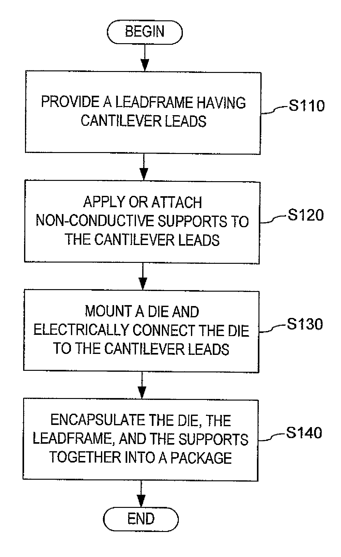
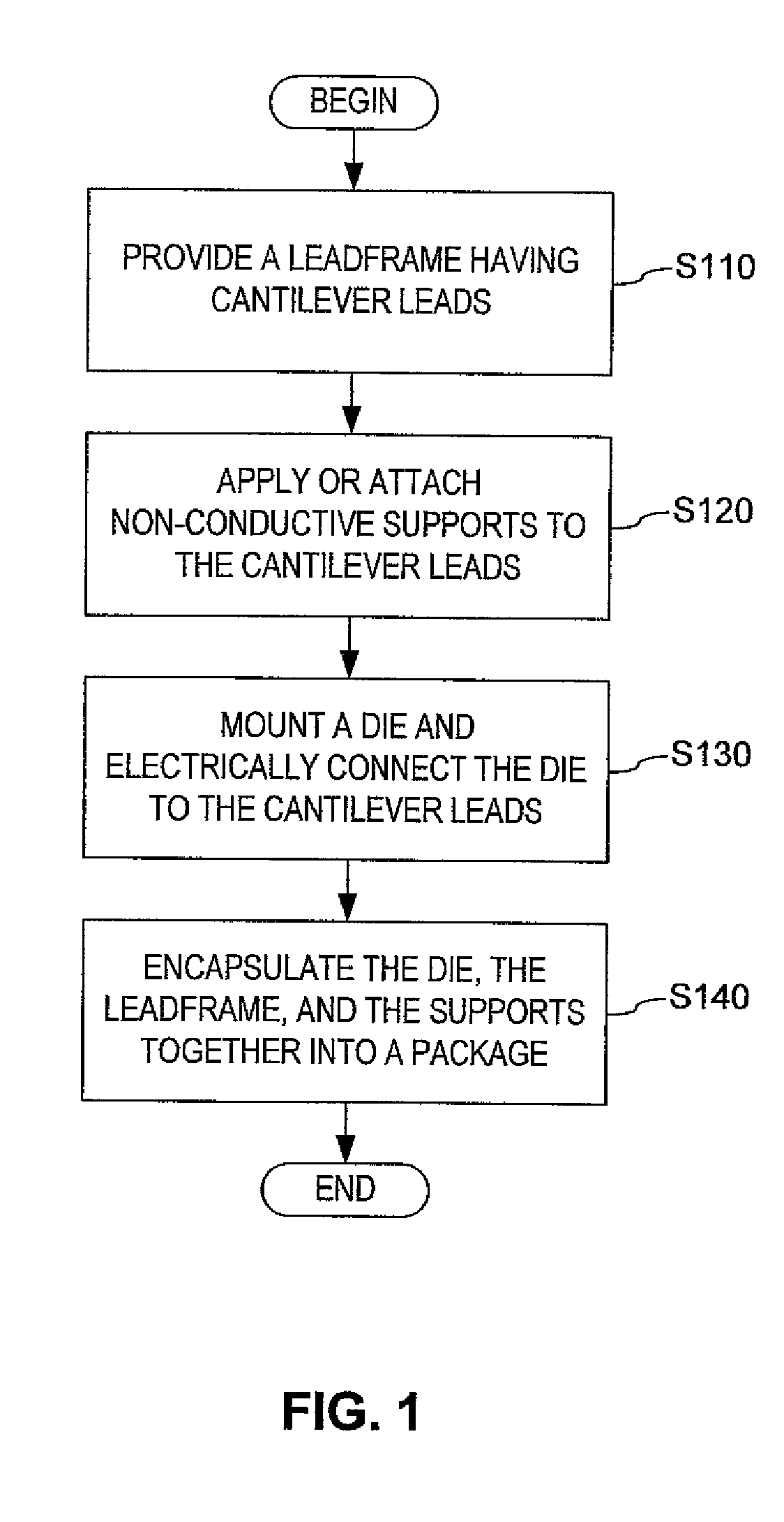
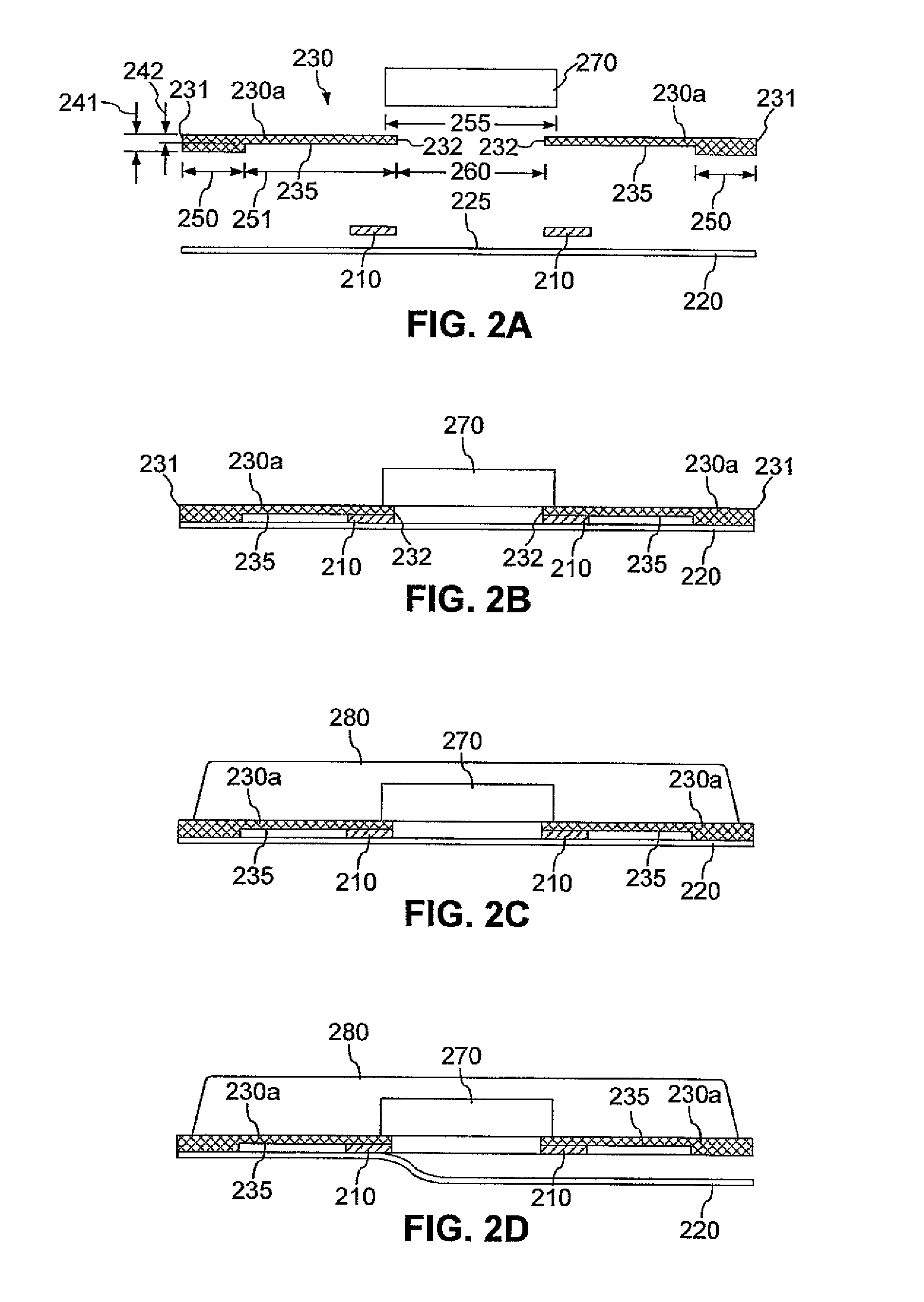
[0020]Reference will now be made in detail to the exemplary embodiments, an example of which is illustrated in the accompanying drawings. Wherever possible, the same reference numbers will be used throughout the drawings to refer to the same or like parts.

[0021]In the following description, reference is made to the accompanying drawings that form a part thereof, and in which is shown by way of illustration specific exemplary embodiments in which may be practiced. These embodiments are described in sufficient detail to enable those skilled in the art to practice these embodiments and it is to be understood that other embodiments may be utilized and that changes may be made without departing from the scope of the invention. The following description is, therefore, merely exemplary.

[0022]Notwithstanding that the numerical ranges and parameters setting forth the broad scope of the exemplary embodiments are approximations, the numerical values set forth in the specific examples are repor...


PUM


Abstract

A method of manufacturing a semiconductor package includes providing a metallic leadframe having a plurality of cantilever leads and a mounting area for mounting a die, and disposing one or more non-conductive supports adjacent to a recessed surface of the cantilever leads to support the leads during die mount, wire bond, and encapsulation processes. The method further includes mounting the die in the mounting area and electrically connecting the die to the cantilever leads, and then encapsulating at least a portion of the die, the leadframe, and the supports with an encapsulant.

Description

FIELD OF THE INVENTION[0001]This invention relates generally to the field of semiconductor devices and manufacture processes, and more particularly, to methods and devices for manufacturing and supporting cantilever leads in a semiconductor package.DESCRIPTION OF THE RELATED ART[0002]As cellular phones, mobile devices, notebook personal computers, and other miniaturized electronic devices become increasing popular, demands to reduce the size and thickness of semiconductor devices carried therein are greater than ever. These demands have been partially met through the introduction of a family of packaging commonly known as chip scale package (CSP), which has the characteristics of reduced dimensions and weight, simpler assembly process, greater performance, and a general reduction in production costs. A semiconductor package of this type carries the concept of miniaturization to the extreme, as it presents a reduced package footprint, a thin profile, and reduced weight.[0003]A semico...

Claims


Application Information

Patent Timeline
Patent Type & Authority Patents(United States)
IPC IPC(8): H01L21/44
CPCH01L21/568H01L23/4951H01L23/49558H01L23/495H01L23/3107H01L24/48H01L2924/01046H01L2924/18165H01L2224/48247H01L2924/14H01L2924/181H01L2924/00014H01L2924/00H01L2924/00012H01L2224/45099H01L2224/45015H01L2924/207
Inventor HOLLOWAY, JEFFREY GAIL
Owner TEXAS INSTR INC
Why Eureka
Try Eureka