Organic electroluminescence device capable of preventing light from being not emitted

a technology of electroluminescence device and organic material, which is applied in the direction of discharge tube/lamp details, discharge tube luminescnet screen, other domestic articles, etc., can solve the problems of deteriorating display quality, and achieve the effect of low resistance of the second electrod

Active Publication Date: 2012-08-14
ELEMENT CAPITAL COMMERCIAL CO PTE LTD
View PDF10 Cites 0 Cited by
  • Summary
  • Abstract
  • Description
  • Claims
  • Application Information

AI Technical Summary

Benefits of technology

[0015]An advantage of some aspects of the invention is that it provides an organic electroluminescence device capable of preventing light from being not emitted due to step disconnection (line disconnection) caused by a step difference in a partition wall and ensuring a satisfactory display quality.
[0017]According to the organic electroluminescence device, the second electrode is formed in the area where both the formation area of the organic electroluminescence element and the non-formation area of the organic electroluminescence element overlap with each other, so as to be electrically connected to the function layer and the auxiliary electrode and is formed continuously between the function layer arranged within the concave portion and the auxiliary electrode in the state where the second electrode contacts with the function layer arranged within the concave portion and the auxiliary electrode. Accordingly, even when step disconnection occurs in the second electrode due to a step difference of the partition wall, the second electrode contacts with the auxiliary electrode formed within the concave portion and thus the upper portion of the partition wall causing the step disconnection is conductively connected to the inside of the concave portion through the auxiliary electrode. Since the second electrode contact with the function layer arranged within the concave portion, sufficient current flows in the function layer of the formation area of the organic electroluminescence element, thereby realizing satisfactory light emission. In addition, since the auxiliary electrode is thicker than the second electrode, the step disconnection rarely occurs due to the step difference of the partition wall. As a result, the organic electroluminescence device can prevent the light from being not emitted due to the step disconnection (line disconnection) caused due to the step difference of the partition wall and can realize a high display quality.
[0027]With such a configuration, resistance obtained by a sum of the resistances of the second electrode and the auxiliary electrode can be lowered. Accordingly, it is possible to realize substantially low resistance of the second electrode and remove the display unevenness.
[0029]With such a configuration, even when the height of the partition wall is in the range of about 1 to 3 μm, the step disconnection (line disconnection) can be prevented from occurring in the auxiliary electrode due to the step difference of the partition wall.
[0031]By forming the auxiliary electrode by the mask vapor-deposition method, it is possible to form the auxiliary electrode in a desired pattern without damage to the function layer which is caused by etching.
[0033]Since the resistance of Al is low and the film can be formed by vapor deposition, it is possible to realize substantially low resistance of the second electrode and form the film in a desired pattern by the mask vapor-deposition method.

Problems solved by technology

Therefore, in a case of a large-scale organic EL display (organic EL device), since irregularity of brightness between the organic EL elements is caused in the outer circumference and the inside of a display area, for example, due to a voltage drop of the cathode resulting from the increased resistance value, a problem may occur in that a display quality deteriorates due to display unevenness such as light emission unevenness or bright unevenness.

Method used


Image

  • Organic electroluminescence device capable of preventing light from being not emitted
  • Organic electroluminescence device capable of preventing light from being not emitted
  • Organic electroluminescence device capable of preventing light from being not emitted

Examples


first embodiment

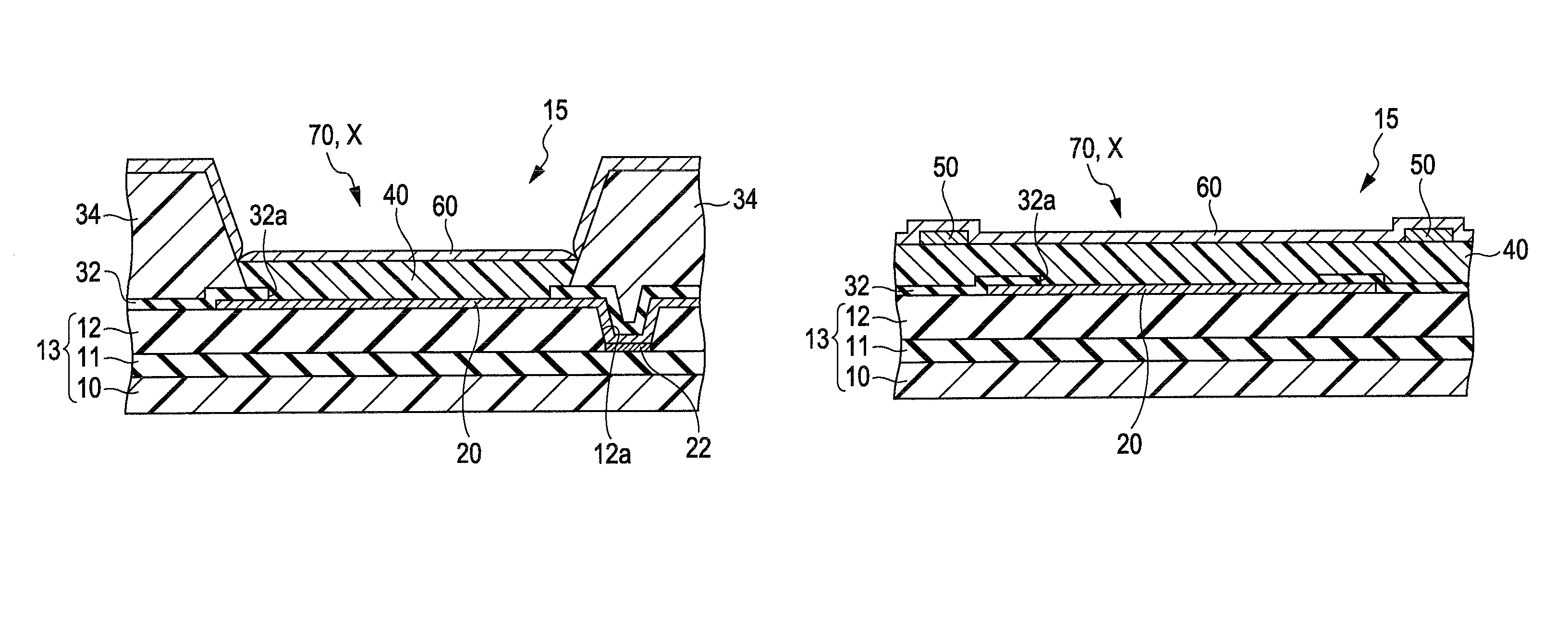
[0055]Next, a specific configuration example of the organic EL device will be described with reference to a first embodiment of the invention. FIG. 3 is an enlarged top view illustrating major constituent elements of the organic EL device according to the first embodiment of the invention. FIG. 4A is a sectional view taken along the line IVA-IVA of FIG. 3. FIG. 4B is a sectional view taken along the line IVB-IVB of FIG. 3. FIG. 4C is a sectional view taken along the line IVC-IVC of FIG. 3.

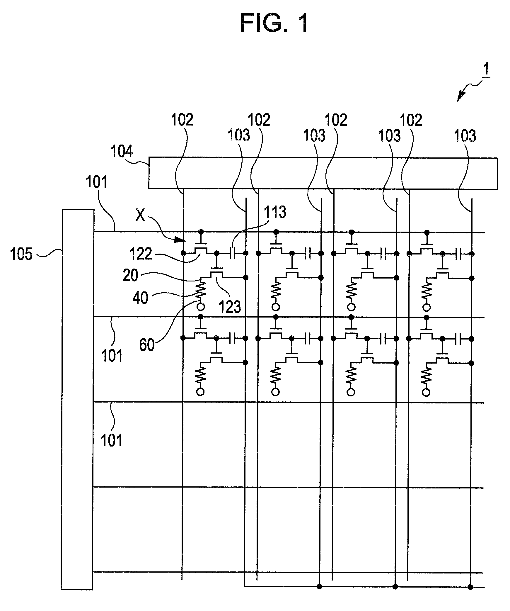
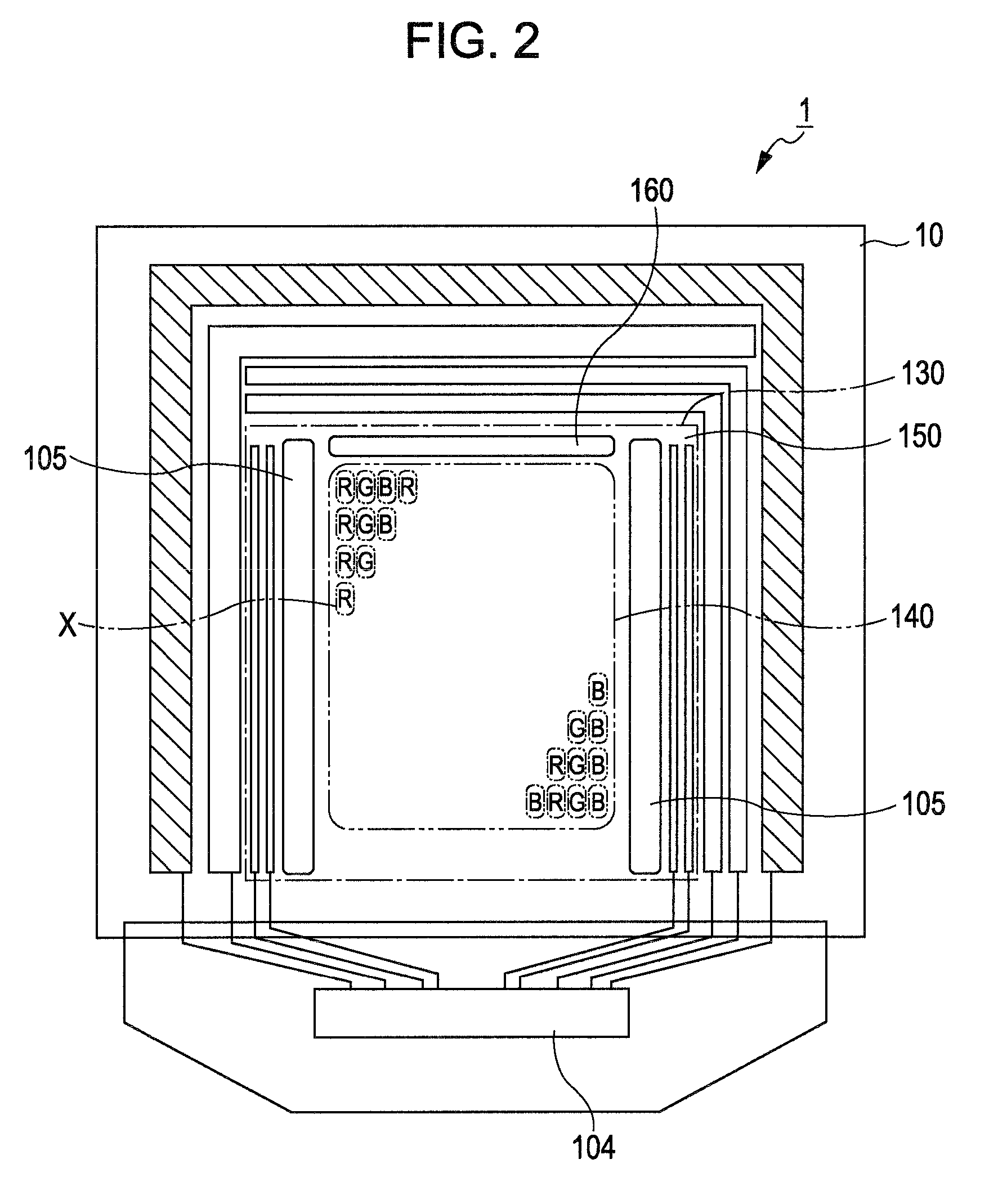
[0056]In the organic EL device 1 according to this embodiment, as shown in FIG. 3, numerous partition walls 34 are arranged in a stripe shape. Each of concave portions 15 is formed between the adjacent partition walls 34. Numerous auxiliary cathode wires (auxiliary electrodes) 50 perpendicular (intersected) to the partition walls 34 are arranged in a stripe shape. Here, the stripe shape includes a shape in which the numerous partition walls 34 are connected to each other in ends or numerous auxilia...

second embodiment

[0086]Next, an organic EL device will be described according to a second embodiment of the invention, FIG. 5 is an enlarged top illustrating major constituent elements of the organic EL device according to the second embodiment of the invention. FIG. 6A is a sectional view taken along the line VIA-VIA of FIG. 5. FIG. 6B is a sectional view taken along the line VIB-VIB of FIG. 5. FIG. 6C is a sectional view taken along the line VIC-VIC of FIG. 5.

[0087]A difference between the organic EL device according to this embodiment shown in FIG. 5 and the organic EL device according to the first embodiment in FIG. 3 is the configurations of the partition wall, the concave portion formed by the partition wall, and the auxiliary cathode wire.

[0088]That is, in the organic EL device according to this embodiment, as shown in FIG. 5, the partition walls 34 are constituted by first partition walls 34a and second partition walls 34b. In addition, the concave portions 15 formed on the sides of the firs...

third embodiment

[0101]Next, an organic EL device will be described according to a third embodiment of the invention. FIG. 7 is an enlarged top illustrating major constituent elements of the organic EL device according to the third embodiment of the invention. FIG. 8A is a sectional view taken along the line VIIIA-VIIIA of FIG. 7. FIG. 8B is a sectional view taken along the line VIIIB-VIIIB of FIG. 7. FIG. 8A is a sectional view taken along the line VIIIC-VIIIC of FIG. 7.

[0102]A difference between the organic EL device according to this embodiment shown in FIG. 7 and the organic EL device according to the first embodiment in FIG. 3 is the configurations of the partition wall, the concave portion formed by the partition wall, and the auxiliary cathode wire.

[0103]That is, in the organic EL device according to this embodiment, as shown in FIG. 7r the partition walls 34 are not arranged in the stripe shape, but arranged horizontally and vertically in a lattice shape. Each of portions surrounded by the p...


PUM


Abstract

An organic electroluminescence device includes an organic electroluminescence element having a function layer interposed between a first electrode and a second electrode. The function layer includes at least an organic light emission layer. The electroluminescence device includes: partition walls which define concave portions and each of formation areas of the organic electroluminescence element within each of the concave portions to arrange the function layer within the concave portion; and auxiliary electrodes which are each arranged continuously on the partition wall and within the concave portion. The second electrode is formed in an area where both the formation area of the organic electroluminescence element and a non-formation area of the organic electroluminescence element overlap with each other, so as to be electrically connected to the function layer and the auxiliary electrode and is formed continuously between the function layer arranged within the concave portion and the auxiliary electrode in a state where the second electrode contacts with the function layer arranged within the concave portion and the auxiliary electrode. The auxiliary electrode is formed to be thicker than the second electrode.

Description

BACKGROUND[0001]1. Technical Field[0002]The present invention relates to an organic electroluminescence device.[0003]2. Related Art[0004]In recent years, a demand for flat display devices which consume less electric power and have a lighter weight has increased with an advance in diverse information apparatuses. As one of the flat display devices, an organic electroluminescence device (organic EL device) which performs a display by allowing an organic electroluminescence element (organic EL element) which has a function layer including an organic light emission layer to emit light was suggested.[0005]The organic EL device is classified into two display types, that is, a so-called top emission type in which light emitted by the organic EL element is radiated in a side opposite a substrate for forming the organic EL element and a so-called bottom emission type in which the light emitted by the organic EL element is radiated in a substrate for forming the organic EL element by transmit...

Claims


Application Information

Patent Timeline
Patent Type & Authority Patents(United States)
IPC IPC(8): H01J1/62H01J63/04
CPCH01L51/5221H01L27/3246H10K59/122H10K59/80522Y10S428/917H10K59/351H10K50/824
Inventor CHINO, YUJIAKAGAWA, SUGURU
Owner ELEMENT CAPITAL COMMERCIAL CO PTE LTD
Why Eureka
Try Eureka