
Display apparatus

a technology of display apparatus and display screen, which is applied in the direction of solid-state devices, semiconductor devices, organic semiconductor devices, etc., can solve the problems of negative affecting the perceived quality of the displayed image, and achieve the effect of satisfying the display quality

Active Publication Date: 2020-12-08
SAMSUNG DISPLAY CO LTD
View PDF12 Cites 0 Cited by
  • Summary
  • Abstract
  • Description
  • Claims
  • Application Information

AI Technical Summary

Benefits of technology

[0005]Embodiments may be related to a display apparatus with optimized reflectance and satisfactory display quality.
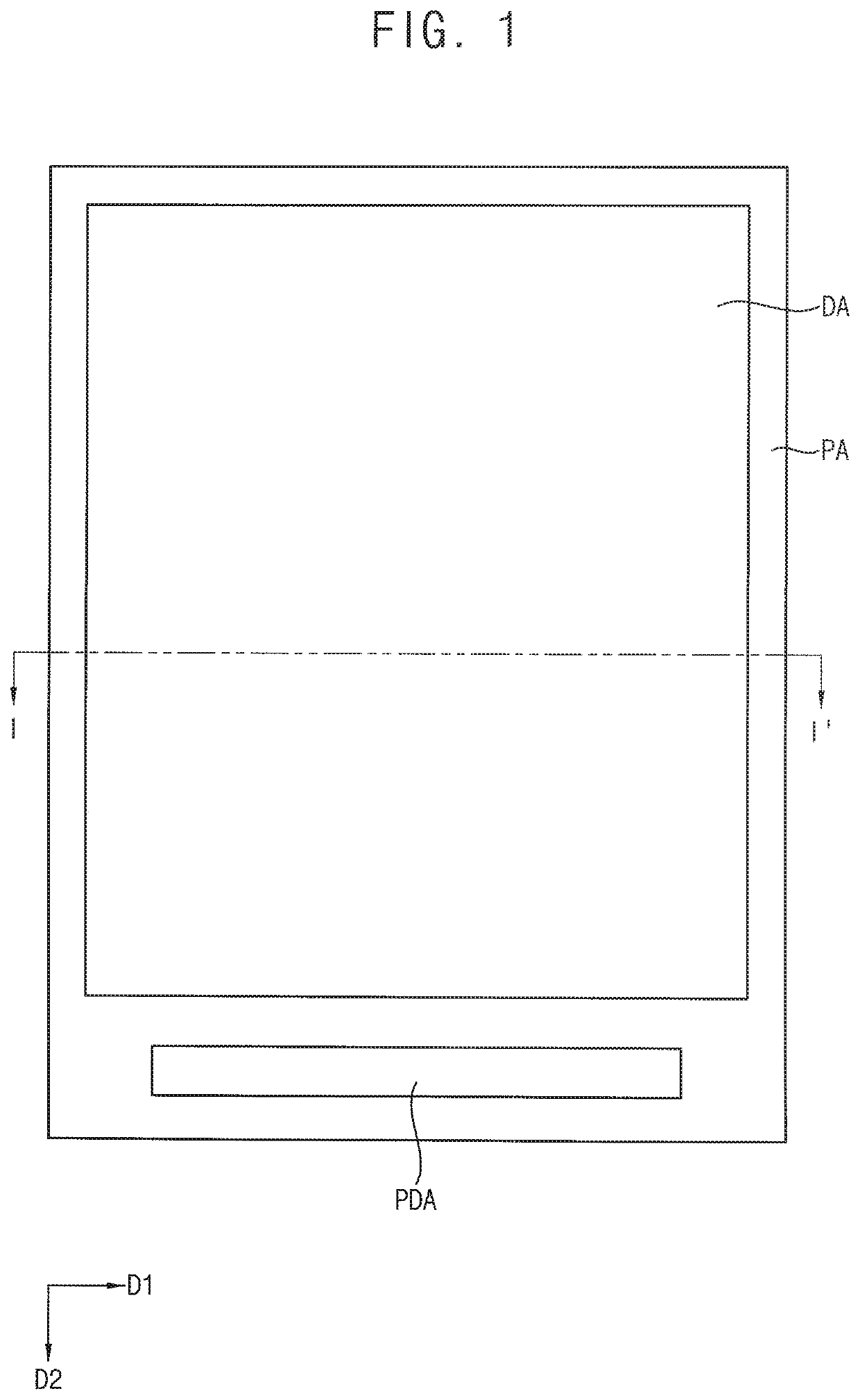
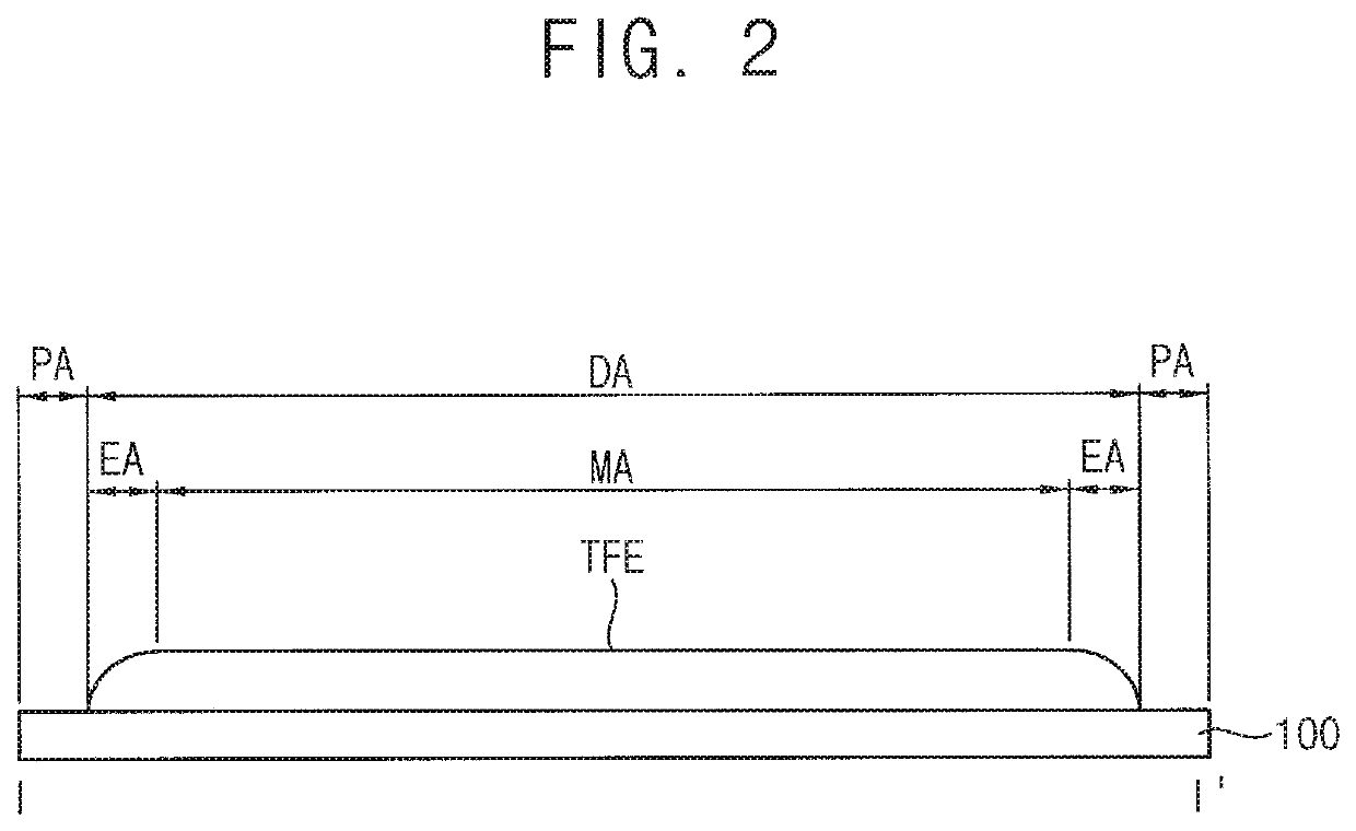
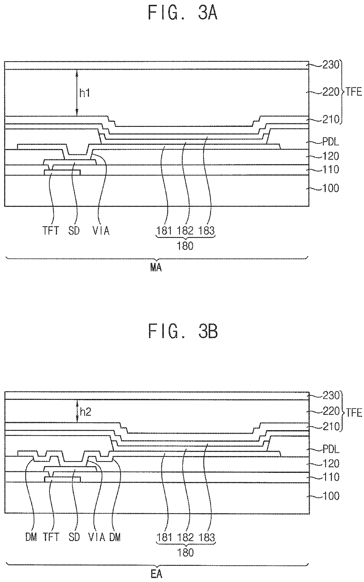
[0025]According to the embodiments of the present inventive concept, a display apparatus includes a display area in which an image is displayed and a peripheral area. The display area includes an edge area and a middle area. In the middle area, an organic layer of a thin-film encapsulation layer has a first height on the via hole. The organic layer in the edge area has a second height smaller than the first height on the via hole. A dummy pattern may be formed in the edge area or a size (width) and a depth (height) of the via hole in the edge area may be different from that in the middle area to compensate for a reflectance deviation. Accordingly, it is possible to easily control the deviation of the reflectance simply by forming a dummy pattern around the via hole without a special additional process.

Problems solved by technology

Significantly inconsistent reflection in different portions of the display area may negatively affect the perceived quality of the displayed image.

Method used


Image

  • Display apparatus
  • Display apparatus
  • Display apparatus

Examples


Embodiment Construction

[0061]Example embodiments are explained with reference to the accompanying drawings.

[0062]Although the terms “first,”“second,” etc. may be used herein to describe various elements, these elements, should not be limited by these terms. These terms may be used to distinguish one element from another element. Thus, a first element may be termed a second element without departing from teachings of one or more embodiments. The description of an element as a “first” element may not require or imply the presence of a second element or other elements. The terms “first,”“second,” etc. may also be used herein to differentiate different categories or sets of elements. For conciseness, the terms “first,”“second,” etc. may represent “first-type (or first-set),”“second-type (or second-set),” etc., respectively.

[0063]The term “dummy pattern” may mean “recessed structure” or “hole.” The term “SD pattern” may mean “drain electrode.” The term “thin film transistor” may mean “semiconductor member.” Th...


PUM

PropertyMeasurementUnit
edge areaaaaaaaaaaa
thicknessaaaaaaaaaa
heightaaaaaaaaaa

Abstract

A display apparatus includes a first transistor, a first pixel electrode, a second transistor, and a second pixel electrode. The first transistor includes a first drain electrode. The first pixel electrode is positioned between an edge of the display apparatus and a center of the display apparatus and includes a first recessed structure. The first recessed structure directly contacts the first drain electrode. The second transistor includes a second drain electrode. The second pixel electrode is positioned between the edge of the display apparatus and the first pixel electrode and includes at least one recessed structure. The at least one recessed structure includes a second recessed structure. The second recessed structure directly contacts the second drain electrode. A total maximum width of the at least one recessed structure is greater than a maximum width of the first recessed structure.

Description

[0001]This application claims priority to and the benefit of Korean Patent Application No. 10-2018-0135070, filed on Nov. 6, 2018 in the Korean Intellectual Property Office; the content of the Korean Patent Application in its entirety is incorporated herein by reference.BACKGROUND1. Field[0002]The technical field relates to a display apparatus.2. Description of the Related Art[0003]Modern display apparatuses may include plasma display apparatuses, liquid crystal display apparatuses, and organic light emitting display apparatuses. A modern display device may have advantages of small size, light weight, and low-power-consumption.[0004]A display apparatus may include a display area for displaying an image. Significantly inconsistent reflection in different portions of the display area may negatively affect the perceived quality of the displayed image.SUMMARY[0005]Embodiments may be related to a display apparatus with optimized reflectance and satisfactory display quality.[0006]One or m...

Claims


Application Information

Patent Timeline
Patent Type & Authority Patents(United States)
IPC IPC(8): H01L27/32H01L51/00H01L51/52
CPCH01L27/3248H01L51/5253H01L51/0097H01L27/3246H01L27/3258H01L2251/5338H10K59/50H10K59/12H10K59/131H10K50/84H10K50/8445H10K50/844Y02E10/549H10K59/123H10K59/124H10K59/351H10K59/1213H10K50/00H10K59/122H10K77/111H10K2102/311
Inventor LEE, EONJOOKIM, HYOENG-KIPARK, KWANGWOOLEE, DONGKIJUNG, JIN-WHAN
Owner SAMSUNG DISPLAY CO LTD
Learn More