Semiconductor device and method of manufacturing the same

a technology of semiconductors and semiconductors, applied in the direction of semiconductor devices, basic electric elements, electrical equipment, etc., can solve the problems of unstable capacitor value, fluctuation of capacitance value, characteristics change, etc., and achieve stable capacitance value, less chance of reliability degradation, and increase the effect of capacitan

Active Publication Date: 2012-08-21
ABLIC INC
View PDF1 Cites 2 Cited by
  • Summary
  • Abstract
  • Description
  • Claims
  • Application Information

AI Technical Summary

Benefits of technology

[0020]An object of the present invention is therefore to provide a semiconductor capacitor that can be formed without high temperature heat treatment and that has less chance of reliability degradation while being stable in capacitance value and capable of increasing the capacitance as in conventional trench capacitors, and to provide a method of manufacturing the semiconductor capacitor.
[0026]The present invention provides a semiconductor capacitor that can be formed without high temperature heat treatment and that has less chance of reliability degradation while being stable in capacitance value and capable of increasing the capacitance as in conventional trench capacitors, and a method of manufacturing the semiconductor capacitor, by applying local oxidation of silicon (LOCOS), which is an existing device isolation technology, and forming a LOCOS trench substrate.

Problems solved by technology

A drawback of planar capacitors is that the capacitance value is unstable because the width of a depletion layer on the surface of the lower electrode layer is varied depending on the input voltage, and the variations in depletion layer width lead to fluctuations in capacitance value.
A problem of stacked capacitors lies in how the capacitor insulating film is formed on polycrystalline silicon.
On the other hand, in thermal oxidation at a high temperature, heat during the oxidation process diffuses impurities, which can cause a characteristics change and decreased reliability in other devices (such as transistor).
However, an oxide film formed by CVD is inferior in characteristics to a thermal oxide film formed on single-crystal silicon.
This means that PIP stacked capacitors cannot have a thin capacitor insulating film because forming a thin oxide film by CVD causes deterioration in withstand voltage and reliability.
PIP stacked capacitors consequently have a drawback in that the capacitance value cannot be increased.
Trench capacitors can consequently suppress a change in capacitance value due to a change in input voltage, which is a problem of planar capacitors.
The resultant drawback is that trench capacitors are susceptible to dielectric breakdown due to field concentration around the trench openings and in the trench bottom corners where the capacitor insulating film and the polycrystalline silicon film are thin, and are accordingly lowered in reliability.
However, the method which requires executing once or twice the process of forming an oxide film at a high temperature of 1,000° C. or higher in an oxygen atmosphere and removing the oxide film in order to round trench openings and trench bottoms has a problem in that the high temperature heat treatment makes the substrate susceptible to damage such as dislocation.
Another problem is that the high temperature heat treatment causes re-distribution in an already formed impurity layer and accordingly raises the possibility of increased variation in impurity concentration.

Method used


Image

  • Semiconductor device and method of manufacturing the same
  • Semiconductor device and method of manufacturing the same
  • Semiconductor device and method of manufacturing the same

Examples


Embodiment Construction

[0034]An embodiment of the present invention is described below in detail.

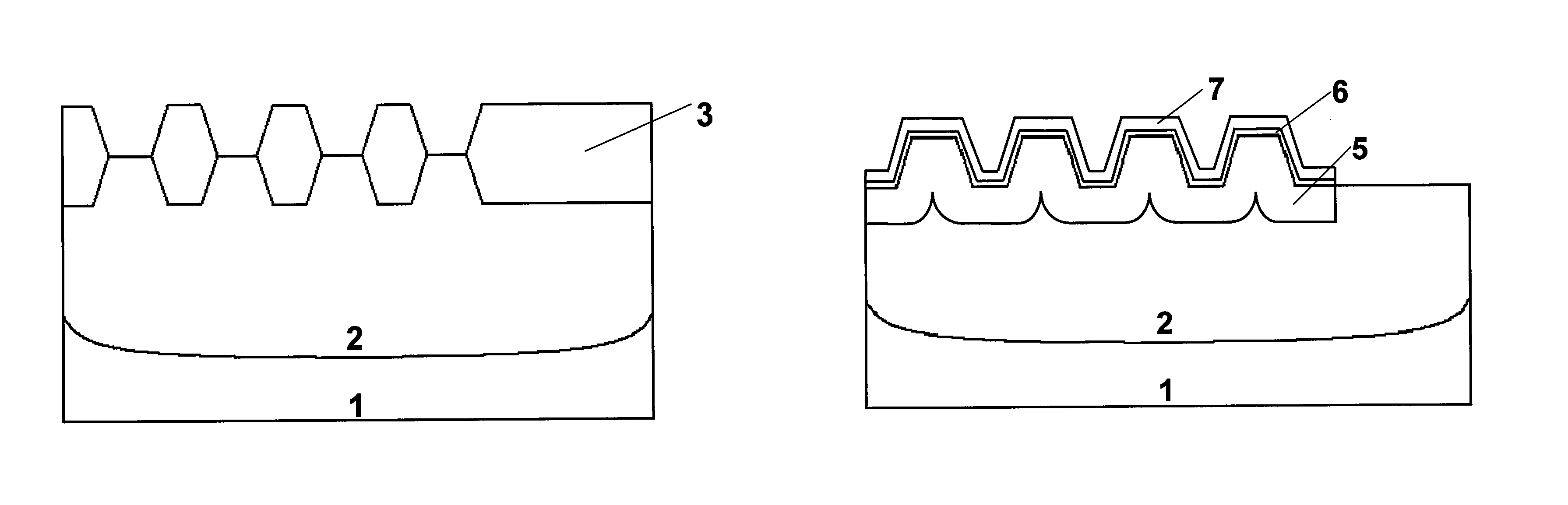
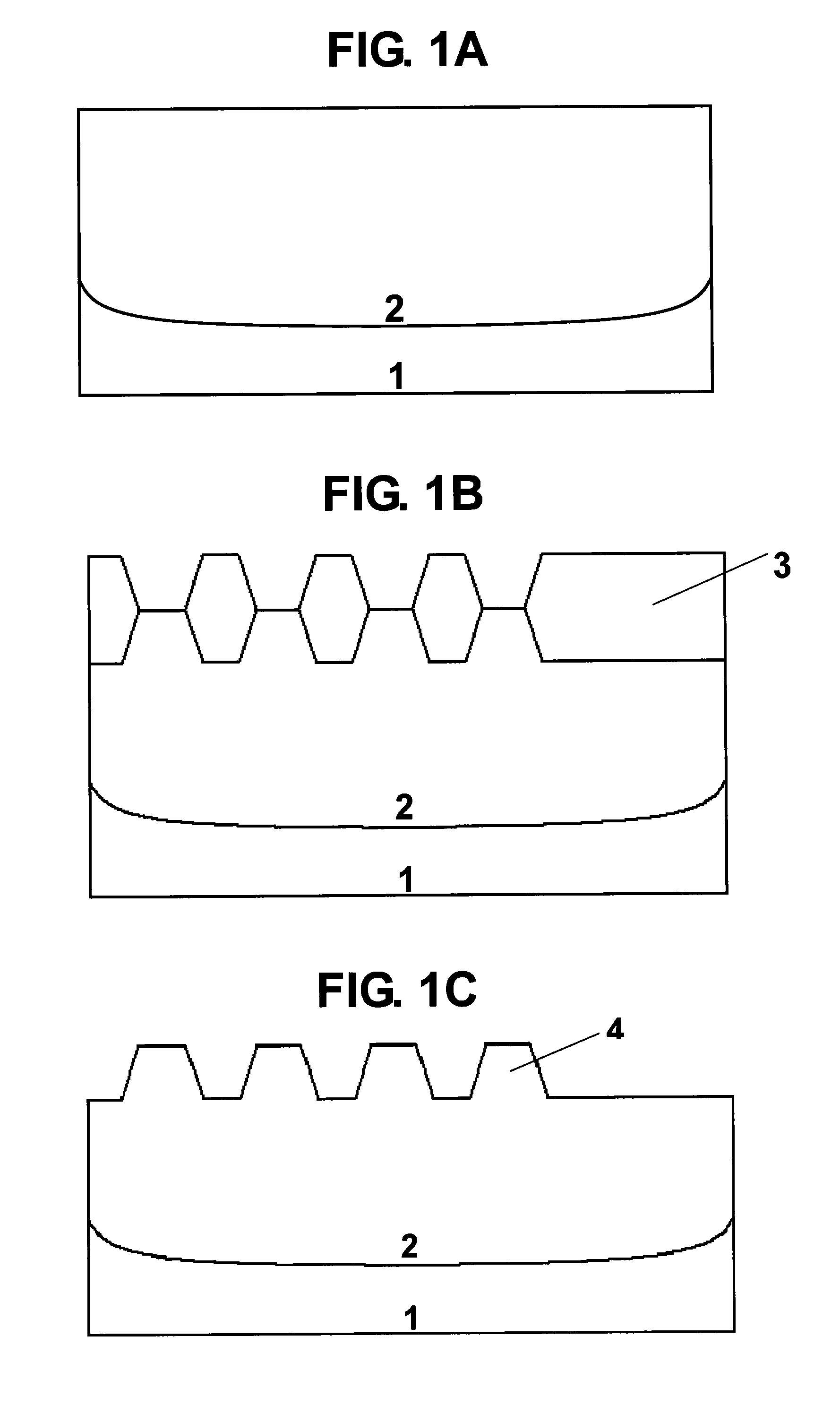
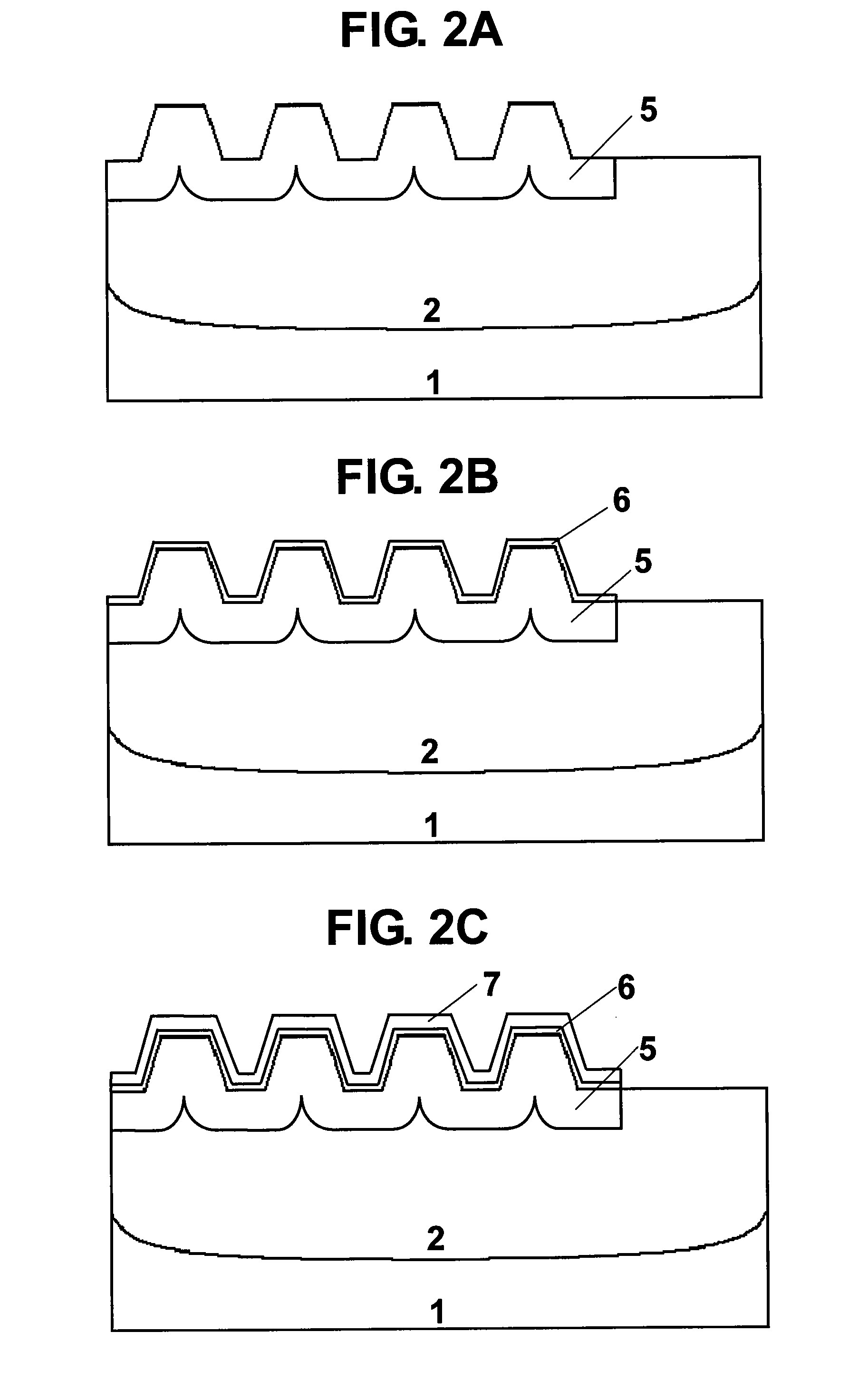
[0035]FIGS. 1A to 1C and FIGS. 2A to 2C are sectional views illustrating manufacturing processes for illustrating a semiconductor device and a method of manufacturing the semiconductor device according to this embodiment. This embodiment takes as an example a capacitor device that uses a P-type semiconductor substrate. However, the essence of the present invention does not depend on the conductivity type of the employed substrate and the type and conductivity type of the employed impurities. The present invention can therefore be carried out the same way as in the embodiment when the conductivity type of the employed substrate and the type and conductivity type of the employed impurities differ from those in the embodiment.

[0036]The structure of the semiconductor device and the method of manufacturing the semiconductor device according to this embodiment are described below with reference to the sectional view...


PUM


Abstract

Provided is a semiconductor capacitor including: a capacitor device forming region having a trapezoidal trench which is formed on a surface of a first conductivity type semiconductor substrate; a second conductivity type lower electrode layer provided along the trapezoidal trenches of the capacitor device forming region; a capacitor insulating film formed at least on a surface of the second conductivity type lower electrode layer; and a second conductivity type upper electrode formed on a surface of the capacitor insulating film.

Description

RELATED APPLICATIONS[0001]This application claims priority under 35 U.S.C. §119 to Japanese Patent Application No. 2010-071085 filed on Mar. 25, 2010, the entire content of which is hereby incorporated by reference.BACKGROUND OF THE INVENTION[0002]1. Field of the Invention[0003]The present invention relates to a semiconductor device including a semiconductor capacitor and a method of manufacturing the semiconductor device.[0004]2. Description of the Related Art[0005]A semiconductor capacitor, which is one of the key components of a semiconductor circuit, is incorporated in various kinds of ICs, and semiconductor capacitors having various structures are used. Conventional semiconductor capacitors include planar capacitors. A typical planar capacitor structure and a method of manufacturing the structure are described for a capacitor formed on a P-type semiconductor substrate as an example with reference to sectional views of FIGS. 3A to 3C illustrating manufacturing processes.[0006]Fi...

Claims


Application Information

Patent Timeline
Patent Type & Authority Patents(United States)
IPC IPC(8): H01L21/20
CPCH01L29/66181H01L29/945
Inventor INOUE, AYAKOSAITOH, NAOTO
Owner ABLIC INC
Why Eureka
Try Eureka