
Reduction of edge effects from aspect ratio trapping

a technology of aspect ratio and edge effect, applied in the direction of solid-state devices, coatings, chemical vapor deposition coatings, etc., can solve the problems of reducing manufacturing yield, requiring additional processes, and reducing device performance, so as to reduce the edge effect of lattice mismatched materials

Active Publication Date: 2012-09-25
TAIWAN SEMICON MFG CO LTD
View PDF481 Cites 73 Cited by
  • Summary
  • Abstract
  • Description
  • Claims
  • Application Information

AI Technical Summary

Benefits of technology

[0007]Embodiments according to the present invention provide methods, structures and apparatus to reduce edge effects of lattice mismatched materials.
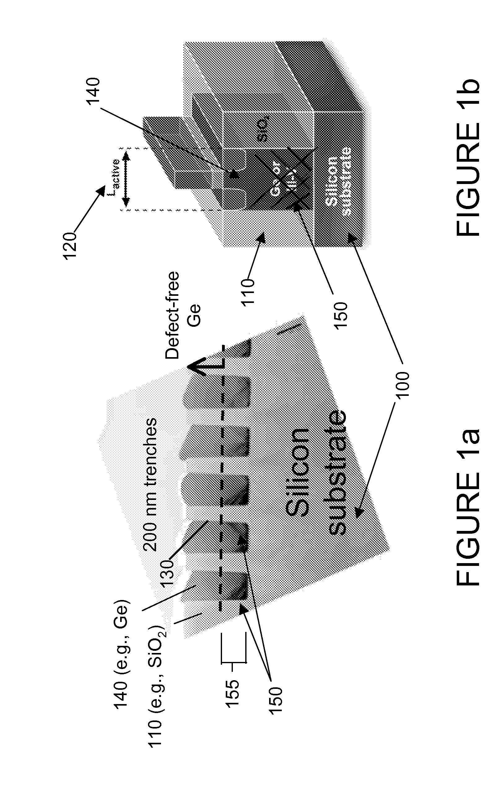
[0008]Embodiments according to the present invention provide methods, structures and apparatus to reduce edge effects or edge related disadvantages of aspect ratio trapping (ART) techniques suitable for device fabrication and / or devices made thereby.
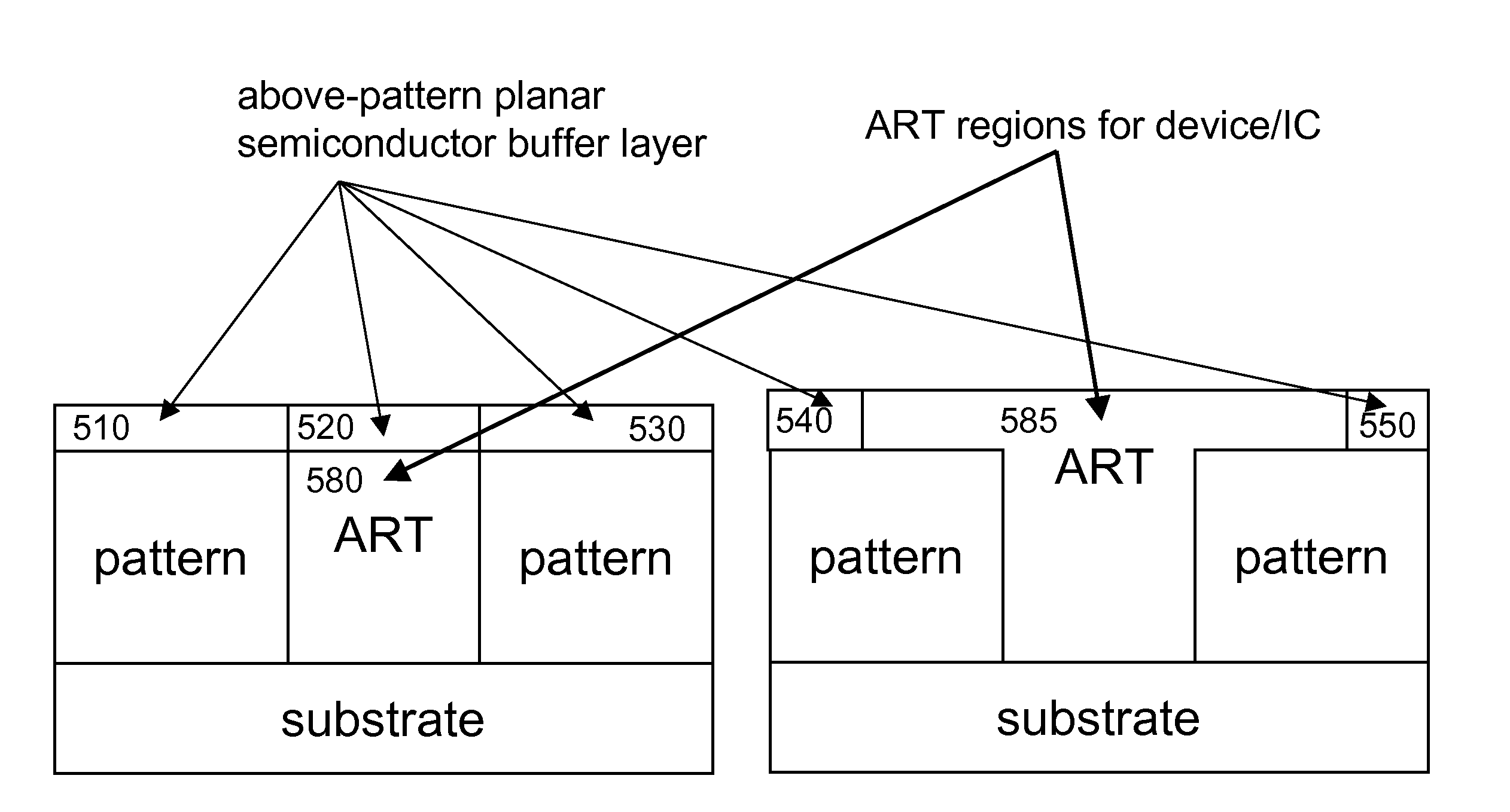
[0009]In one aspect, one embodiment of the invention can provide an above-pattern planar buffer layer to reduce or eliminate effects of physical edges of the heteroepitaxial regions (e.g., Ge regions).
[0010]In another aspect, one embodiment of the invention can provide ART structures with reduced or low levels of edge leakage characteristics and / or surface recombination characteristics.
[0011]In another aspect, one embodiment of the invention can provide ART structures with reduced or low levels of three dimensional feature inaccuracies and / or layer dimension differences.

Problems solved by technology

However, disadvantages associated with structural characteristics of related art lattice mismatched devices can decrease device performance, require additional processes or design constraints to counter-effect such structural characteristics or reduce manufacturing yield.

Method used


Image

  • Reduction of edge effects from aspect ratio trapping
  • Reduction of edge effects from aspect ratio trapping
  • Reduction of edge effects from aspect ratio trapping

Examples


Embodiment Construction

[0027]Reference will now be made in detail to the embodiments of the present general inventive concept, examples of which are illustrated in the accompanying drawings, wherein like reference numerals refer to like elements throughout. The embodiments are described below in order to explain the present general inventive concept by referring to the figures.

[0028]The formation of lattice-mismatched materials has many practical applications. For Example, heteroepitaxially growth of group IV materials or compounds, and III-V, III-N and II-VI compounds on a crystalline substrate, such as silicon has many applications such as photovoltaics, resonant tunneling diodes (RTD's), transistors (e.g., FET (which can be planar or 3D (e.g., finFET), HEMT, etc.), light-emitting diodes and laser diodes. As one example, heteroepitaxy of germanium on silicon is considered a promising path for high performance p-channel metal-oxide-semiconductor (MOS) field-effect transistors (FET) and for integrating op...


PUM

PropertyMeasurementUnit
aspect ratioaaaaaaaaaa
thicknessaaaaaaaaaa

Abstract

A device includes a crystalline material within an area confined by an insulator. In one embodiment, the area confined by the insulator is an opening in the insulator having an aspect ratio sufficient to trap defects using an ART technique. Method and apparatus embodiments of the invention can reduce edge effects in semiconductor devices. Embodiments of the invention can provide a planar surface over a buffer layer between a plurality of uncoalesced ART structures.

Description

RELATED APPLICATIONS[0001]This application claims the benefit of and priority to U.S. Provisional Application No. 61 / 077,462 filed Jul. 1, 2008, inventor Zhiyuan Cheng, entitled “REDUCTION OF EDGE EFFECTS FROM ASPECT RATIO TRAPPING” and U.S. Provisional Application No. 61 / 077,465 filed Jul. 1, 2008, inventor Zhiyuan Cheng, entitled “A SEMICONDUCTOR DEVICE AND METHOD OF MAKING THE SAME”, the disclosure of which is hereby incorporated by reference in its entirety.BACKGROUND OF THE INVENTION[0002]1. Field of the Invention[0003]The present invention relates to semiconductor structures or device fabrication using lattice mismatched materials.[0004]2. Description of the Related Art[0005]This section provides background information and introduces information related to various aspects of the disclosure that are described and / or claimed below. These background statements are not admissions of prior art.[0006]Integration of lattice mismatched semiconductor materials is one path to high perfo...

Claims


Application Information

Patent Timeline
Patent Type & Authority Patents(United States)
IPC IPC(8): H01L21/02
CPCH01L21/8252H01L29/267H01L27/0605H01L29/66462H01L29/04H01L21/8258H01L21/0237H01L21/02532H01L21/02639H01L31/0475Y02E10/50H01L21/02381H01L29/0607H01L29/0649H01L29/32H01L21/02513H01L21/02694
Inventor CHENG, ZHIYUAN
Owner TAIWAN SEMICON MFG CO LTD
Learn More