Method and apparatus for reducing substrate edge effects in electron lenses

a technology of electron lens and substrate edge effect, which is applied in the direction of individual semiconductor device testing, semiconductor/solid-state device testing/measurement, instruments, etc., can solve the problem of not establishing the electrical connection between layers, and achieve the effect of reducing the edge effect of the wafer

Active Publication Date: 2005-06-07
KLA TENCOR TECH CORP
View PDF4 Cites 30 Cited by
  • Summary
  • Abstract
  • Description
  • Claims
  • Application Information

AI Technical Summary

Benefits of technology

[0016]FIG. 7 is a flow chart depicting another method that reduces a wafer edge effect in accordance with an embodiment of the invention.

Problems solved by technology

If one of these holes or vias becomes clogged with non-conductive material, this electrical connection between layers will not be established.

Method used


Image

  • Method and apparatus for reducing substrate edge effects in electron lenses
  • Method and apparatus for reducing substrate edge effects in electron lenses
  • Method and apparatus for reducing substrate edge effects in electron lenses

Examples


Embodiment Construction

[0020]In accordance with one embodiment of the invention, an automated inspection system continuously moves semiconductor wafers under an electron beam. One such system is described, for example, in U.S. Pat. No. 5,973,323, entitled “Apparatus and Method for Secondary Electron Emission Microscope,” inventors Adler et al., and assigned at issuance to KLA-Tencor Corporation of San Jose, Calif. U.S. Pat. No. 5,973,323 is hereby incorporated by reference in its entirety.

[0021]One type of conventional electron inspection system utilizes a combined electrostatic / magnetic cathode objective lens with a strong uniform electric field (few kilovolts per millimeter). Image obtained using such a system has distortions near the edge of a semiconductor wafer being inspected, and the distortion is problematic and disadvantageous.

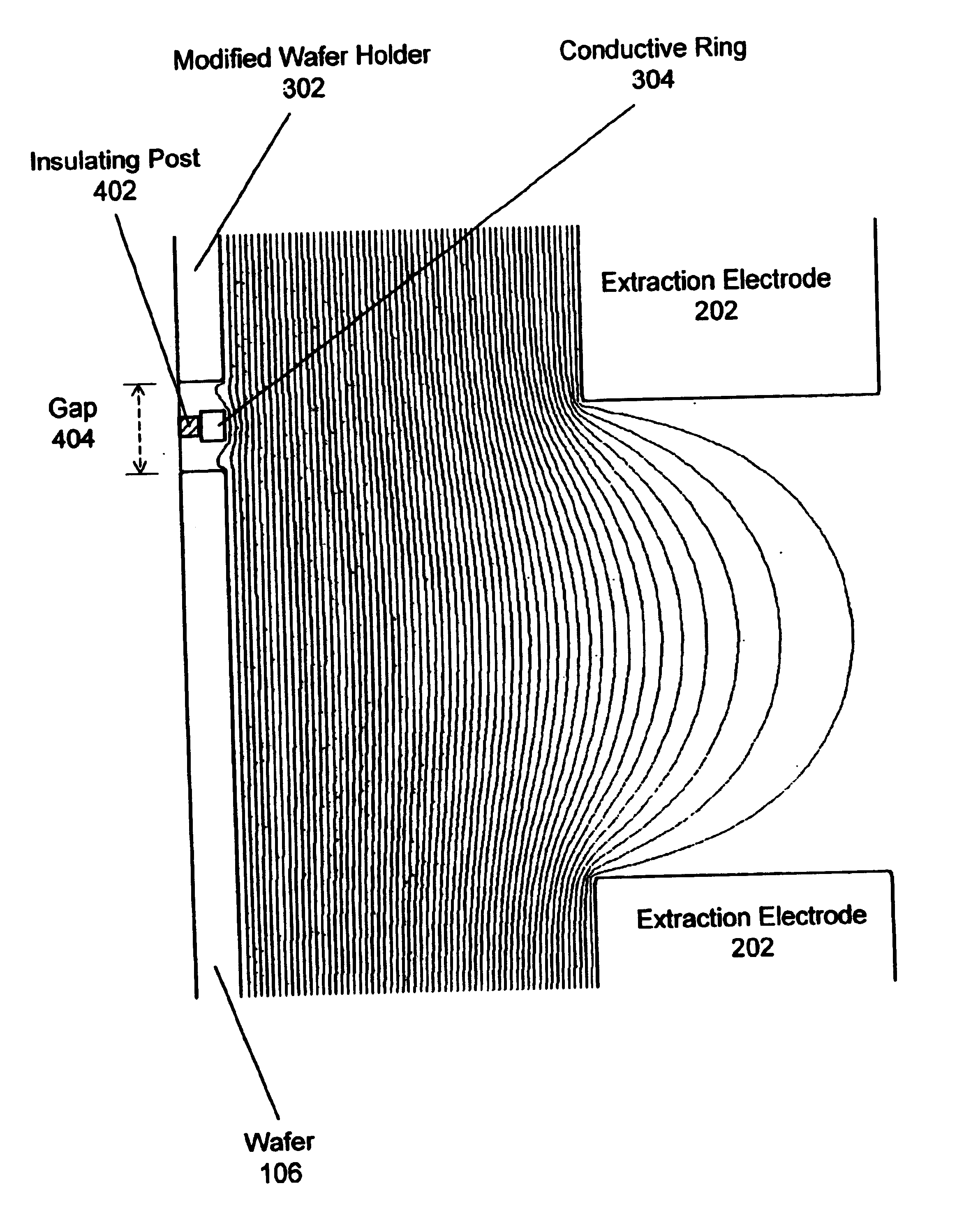
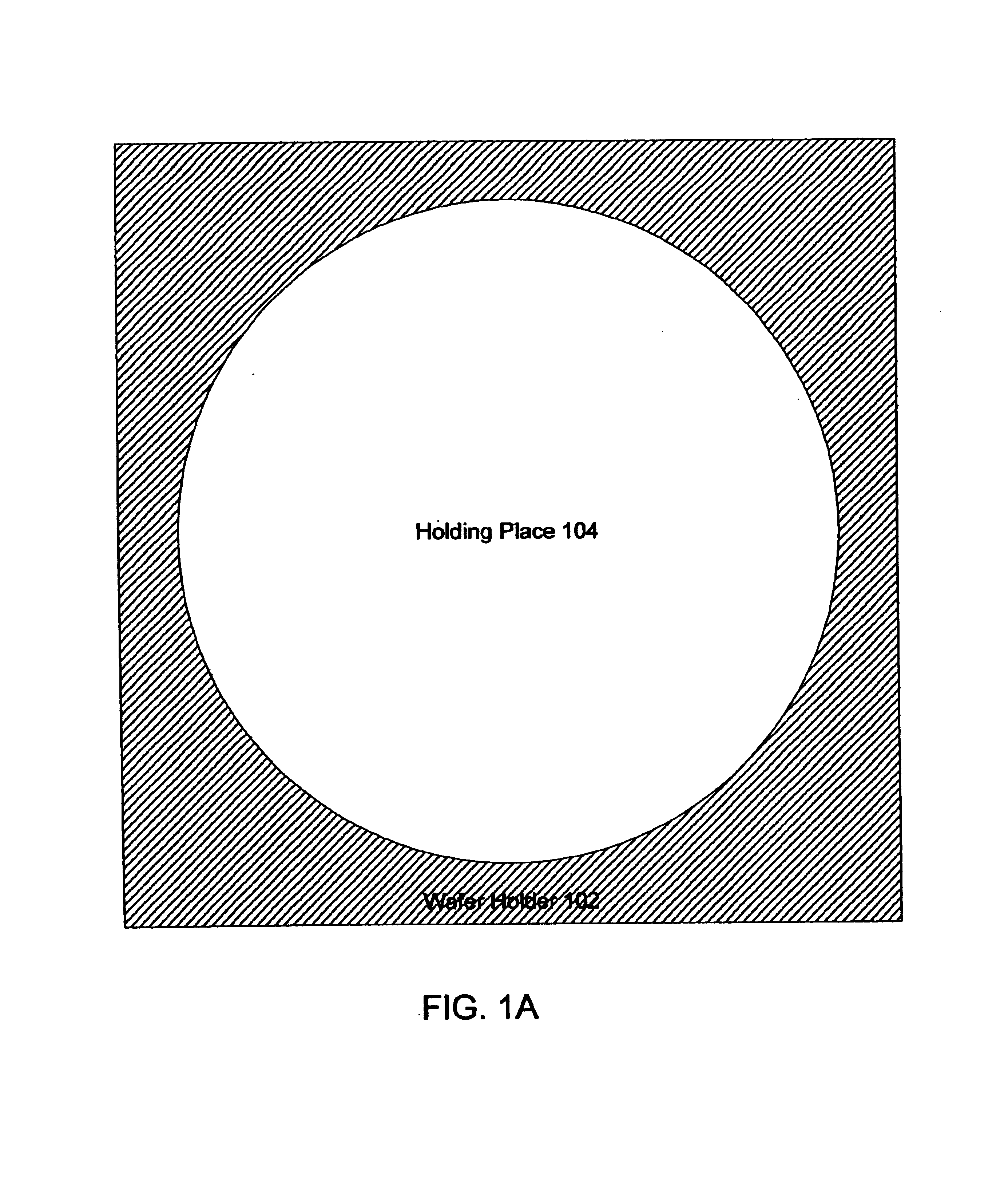
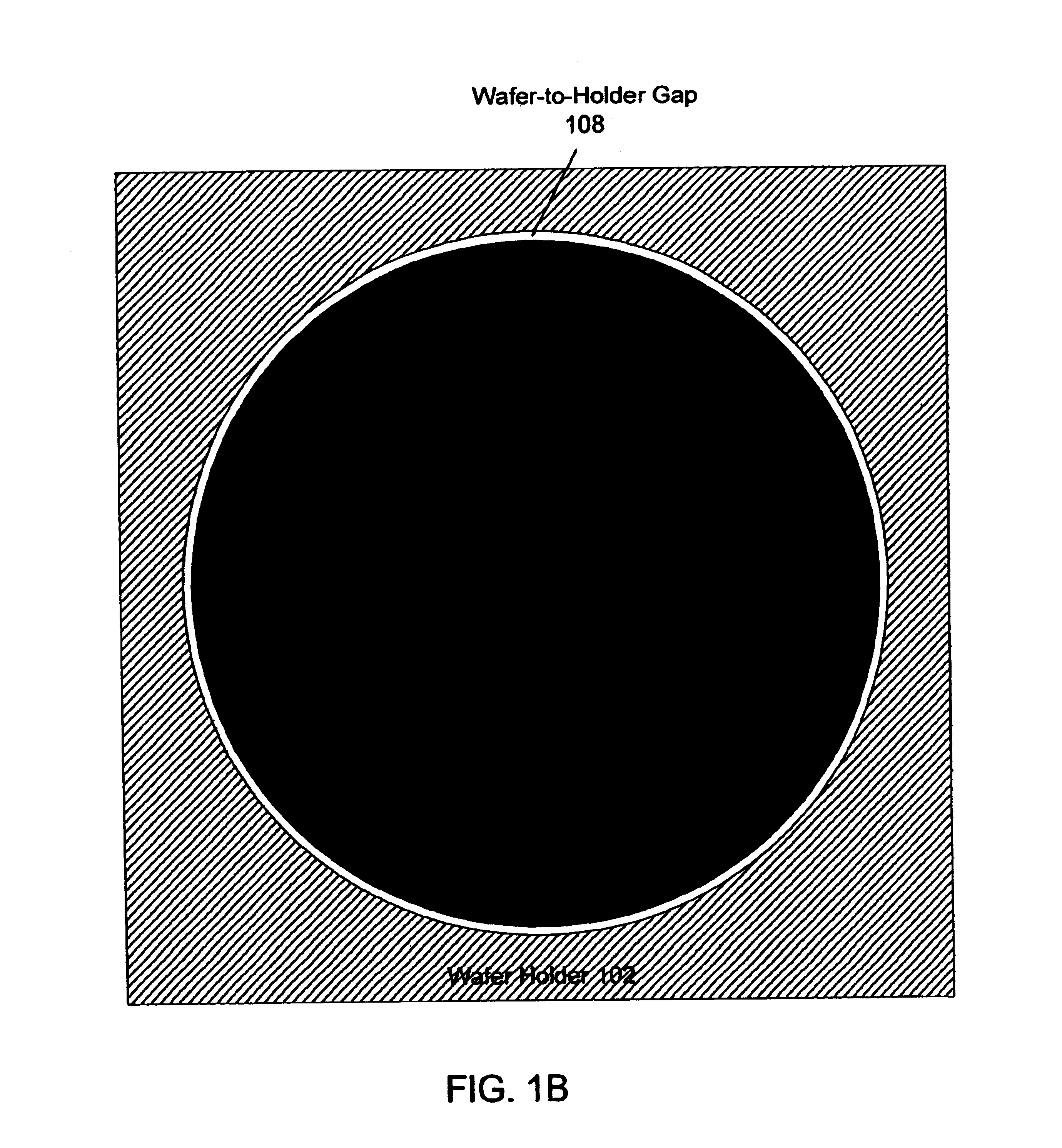
[0022]The present invention identifies a significant source of that distortion as the gap between the wafer edge and the wafer holder. Applicants have determined that this ...


PUM

PropertyMeasurementUnit
voltageaaaaaaaaaa
voltageaaaaaaaaaa
voltageaaaaaaaaaa

Abstract

One embodiment disclosed pertains to a method for inspecting a substrate. The method includes inserting the substrate into a holding place of a substrate holder, moving the substrate holder under an electron beam, and applying a voltage to a conductive element of the substrate holder. The voltage applied to the conductive element reduces a substrate edge effect. Another embodiment disclosed relates to an apparatus for holding a substrate that reduces a substrate edge effect. The apparatus includes a holding place for insertion of the substrate and a conductive element. The conductive element is positioned so as to be located within a gap between an edge of the holding place and an edge of the substrate.

Description

CROSS-REFERENCE TO RELATED APPLICATIONS[0001]The present application claims the benefit of provisional patent application No. 60 / 443,666, filed Jan. 30, 2003, entitled “Method and Apparatus for Reducing Substrate Edge Effects in Electron Lenses”, by inventors Marian Mankos and David L. Adler, the disclosure of which is hereby incorporated by reference.BACKGROUND OF THE INVENTION[0002]1. Field of the Invention[0003]The present invention relates generally to electron beam (e-beam) methods and apparatus. The present invention relates more particularly to automated e-beam inspection systems for semiconductor manufacturing.[0004]2. Description of the Background Art[0005]A variety of methods have been used to examine microscopic surface structures of semiconductors. These have important applications in the field of semiconductor integrated circuit (IC) fabrication, where microscopic defects at a surface layer can make the difference between a properly functioning or non-functioning IC. Fo...

Claims


Application Information

Patent Timeline
Patent Type & Authority Patents(United States)
IPC IPC(8): G01N23/20G01N23/203G21K7/00H01J37/244H01J37/28H01L21/66H01J37/20G01Q30/02G01Q30/20
CPCH01J37/20Y10T428/12528H01J2237/153
Inventor MANKOS, MARIANADLER, DAVID L.
Owner KLA TENCOR TECH CORP
Why Eureka
Try Eureka