SER testing for an IC chip using hot underfill

a technology of ic chips and sub-layers, applied in semiconductor/solid-state device testing/measurement, semiconductor/solid-state device details, instruments, etc., can solve the problem of allowing access by a hand-held radioactive source, emitted trace amounts, and too small chip-to-substrat gap

Inactive Publication Date: 2012-10-16
ALSEPHINA INNOVATIONS INC
View PDF15 Cites 5 Cited by
  • Summary
  • Abstract
  • Description
  • Claims
  • Application Information

AI Technical Summary

Problems solved by technology

In an integrated circuit (IC) chip package, emission of trace amounts of radioactive impurities is one cause of SEUs.
Unfortunately, however, for ICs that use, for example, solder bumps or balls, such as controlled collapsible chip connections (herein referred to as solder bumps), the chip-to-substrate gap is too small (e.g., on the order of 100 microns or less) to allow access by a hand-held radioactive source.
Furthermore, the substrate blocks any access to the semiconductor device by a radioactive source, handheld or otherwise.
Moreover, the range of alpha particles is substantially smaller than the thickness of the substrate, such that the alpha particles emitted from an external source cannot reach the semiconductor device.
Eliminating lead from the solder bumps reduces, but does not eliminate, the alpha radiation to the chip.
In addition, alpha particles from packaging materials, or solder bumps, add to, or compete with, neutron induced soft errors caused by the liberation of charged particles when atmospheric neutrons strike silicon or other materials surrounding the chips.
Disadvantageously, soft errors occur with greater frequency with advances in CMOS and other IC technologies; i.e., as dimensions get smaller, densities increase, and bias voltages become lower.
Furthermore, while soft errors in caches and other static random access memory (SRAM) arrays can be detected and corrected with the aid of error correction codes (ECCs), for example, this is not the case for soft errors in logic circuits.
Unfortunately, therefore, these derating factors are difficult to estimate.
Furthermore, relying on measurements from systems being tested in the field necessitates delays in acquisition of SER information until after the product is made.

Method used


Image

  • SER testing for an IC chip using hot underfill
  • SER testing for an IC chip using hot underfill
  • SER testing for an IC chip using hot underfill

Examples


Embodiment Construction

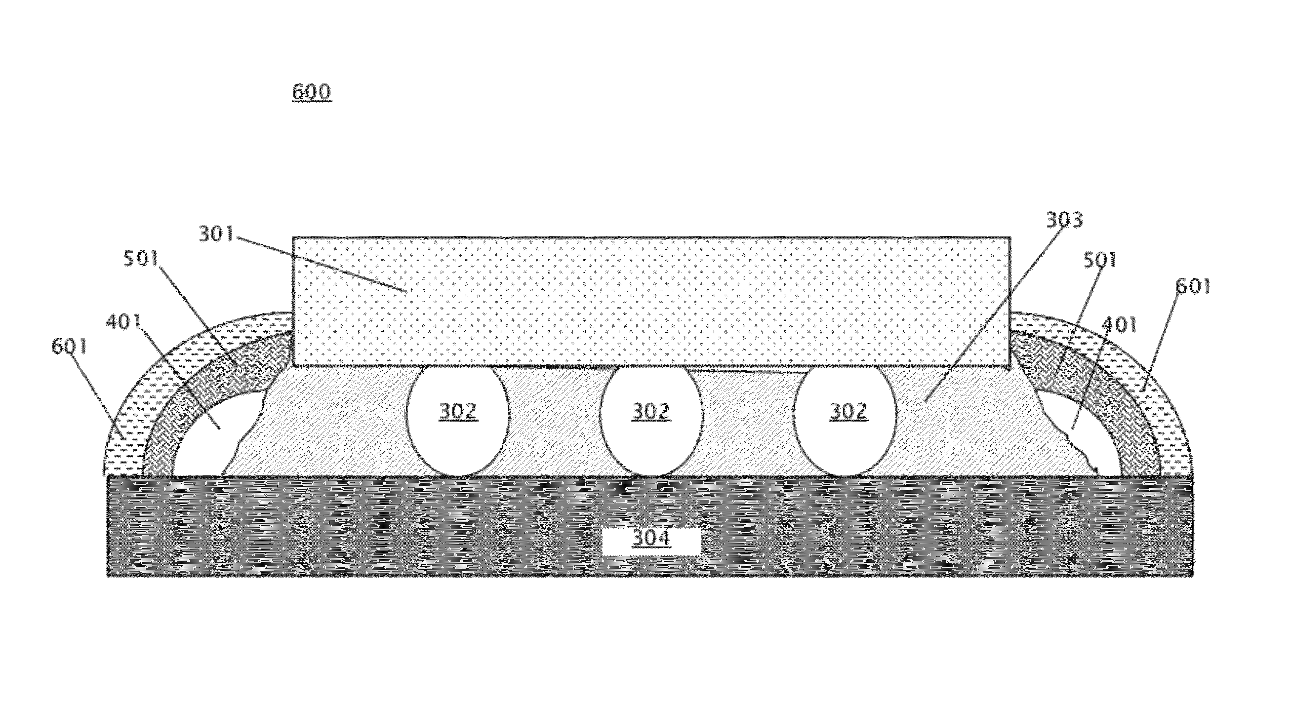
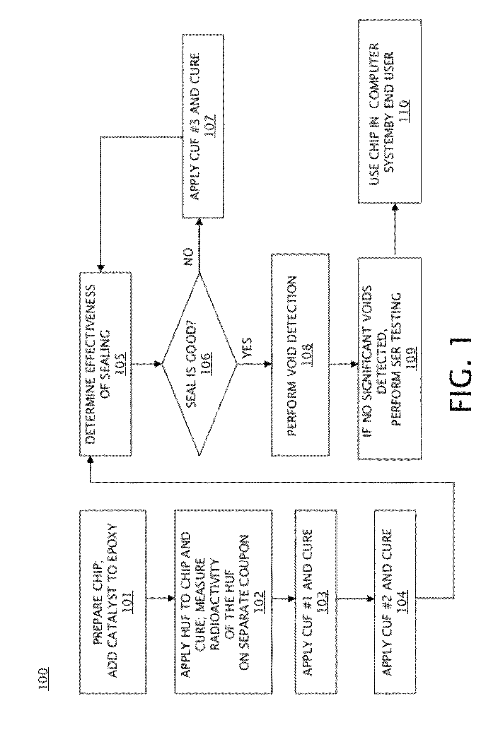
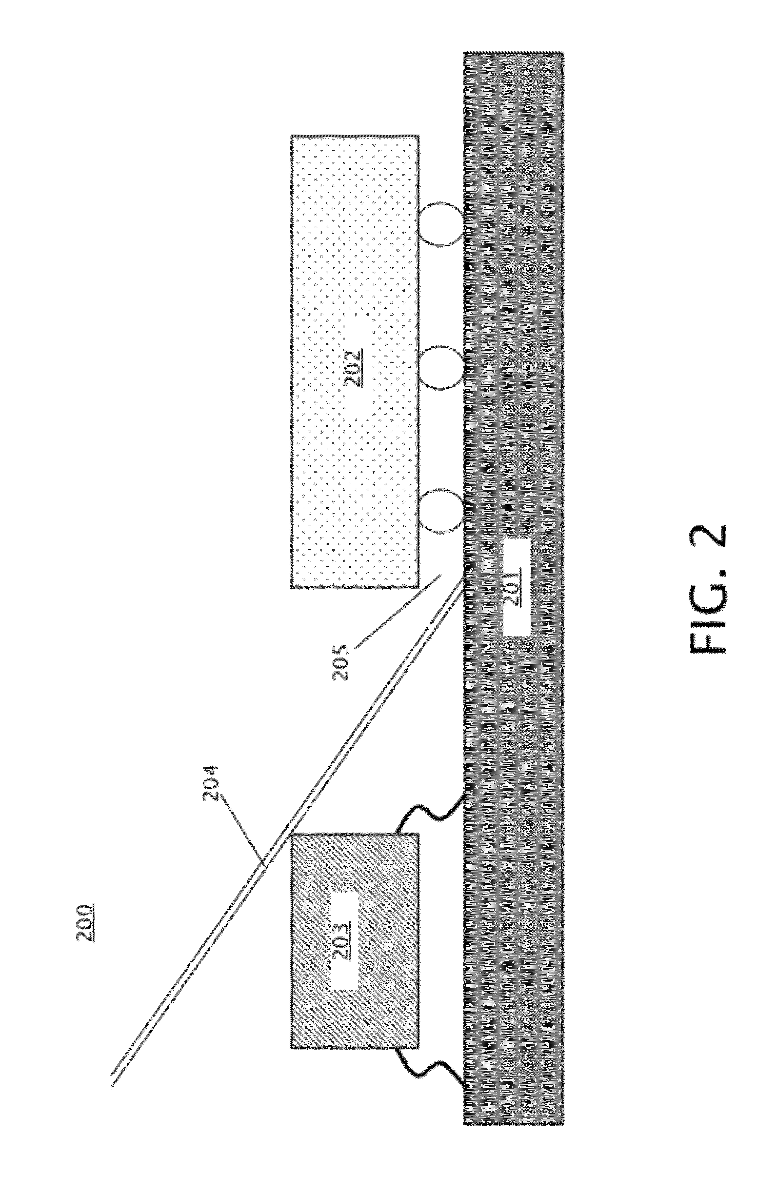
[0017]Embodiments of a method for SER testing for an IC using HUF are provided, with exemplary embodiments being discussed below in detail. Because the half-life of the HUF used for SER testing may be relatively long, proper tracking during SER testing of the HUF chip, and removal and disposal of the HUF chip after testing, may be necessary. Tracking, removal and disposal may add significantly to the cost of the SER testing process. Therefore, to eliminate the needs for tracking, removal, and disposal of the HUF chip, a relatively short-lived isotope may be used for the HUF. After a dozen or so half-lives of the isotope comprising the HUF, which may be days to weeks in some embodiments, the HUF chip is safe to be used in an operational computing device by an end user, with minimal risk of radioactive exposure to the user. The radioactivity of the HUF may be measured right after HUF is applied to the chip by applying it to a test coupon, separate from the chip. Then, using the normal...


PUM


Abstract

A method for detecting soft errors in an integrated circuit (IC) due to transient-particle emission, the IC comprising at least one chip and a substrate includes mixing an epoxy with a radioactive source to form a hot underfill (HUF); underfilling the chip with the HUF; sealing the underfilled chip; measuring a radioactivity of the HUF at an edge of the chip; measuring the radioactivity of the HUF on a test coupon; testing the IC for soft errors by determining a current radioactivity of the HUF at the time of testing based on the measured radioactivity; and after the expiration of a radioactive decay period of the radioactive source, using the IC in a computing device by a user.

Description

FIELD[0001]This disclosure relates generally to the field of detection of soft errors in electronic systems, and, more particularly, to packaging integrated circuits, including logic circuits and array circuits, for accelerated detection of soft error rates due to errors caused by ionizing particle emission.DESCRIPTION OF RELATED ART[0002]Accurate estimates of soft error rates (SERs) in computing devices are desirable for the implementation of reliable systems. Soft errors are caused by single-event upsets (SEUs), which are random, isolated events that may be caused by passage of cosmic rays or transient ionizing particles, such as alpha particles. That is, ionizing particles can generate enough free charge to flip a structure of a memory storage device to its opposite state. In an integrated circuit (IC) chip package, emission of trace amounts of radioactive impurities is one cause of SEUs. For wire-bonded structures, accelerated testing using a radioactive source of alpha particle...

Claims


Application Information

Patent Timeline
Patent Type & Authority Patents(United States)
IPC IPC(8): G01R31/26H01L23/552H01L21/00H01L21/44G01R31/00H01L23/58
CPCG01R31/31816H01L21/563H01L22/20H01L2224/73204H01L2224/32225H01L2924/3511H01L2924/014H01L2224/92125H01L2224/83102H01L2224/16225H01L22/14H01L2924/00
Inventor GAYNES, MICHAELGORDON, MICHAEL S.LABIANCA, NANCY C.LATZKO, KENNETH F.PRABHAKAR, APARNA
Owner ALSEPHINA INNOVATIONS INC
Why Eureka
Try Eureka