Conformal electromagnetic interference shield

a shield and electromagnetic interference technology, applied in the direction of semiconductor/solid-state device details, superimposed coating process, coating, etc., can solve the problems of small and faster electronic devices, and inability to meet the requirements of high clock speed. fast transition between signal levels,

Active Publication Date: 2007-02-08
QORVO US INC
View PDF14 Cites 142 Cited by
  • Summary
  • Abstract
  • Description
  • Claims
  • Application Information

AI Technical Summary

Benefits of technology

[0007] In the first embodiment, an electroless plating process forms a seed layer of conductive material, such as copper (Cu), over the module. The seed layer then carries current for an electrolytic plating process, which deposits a second conductive layer on the seed layer. A third layer may be applied through a second electrolytic plating process. The third layer is a relatively poor conductor compared to the seed layer and the second conductive layer, and may be formed with a material such as ni

Problems solved by technology

While the benefits of these devices are myriad, smaller and faster electronic devices create problems.
In particular, high clock speeds inherently require fast transitions between signal levels.
These electromagnetic emissions radiate from a source and may impinge upon other electronic components.
If the signal strength of the emission at the impinged upon electronic component is hi

Method used


Image

  • Conformal electromagnetic interference shield
  • Conformal electromagnetic interference shield
  • Conformal electromagnetic interference shield

Examples


Embodiment Construction

[0021] The embodiments set forth below represent the necessary information to enable those skilled in the art to practice the invention and illustrate the best mode of practicing the invention. Upon reading the following description in light of the accompanying drawing figures, those skilled in the art will understand the concepts of the invention and will recognize applications of these concepts not particularly addressed herein. It should be understood that these concepts and applications fall within the scope of the disclosure and the accompanying claims.

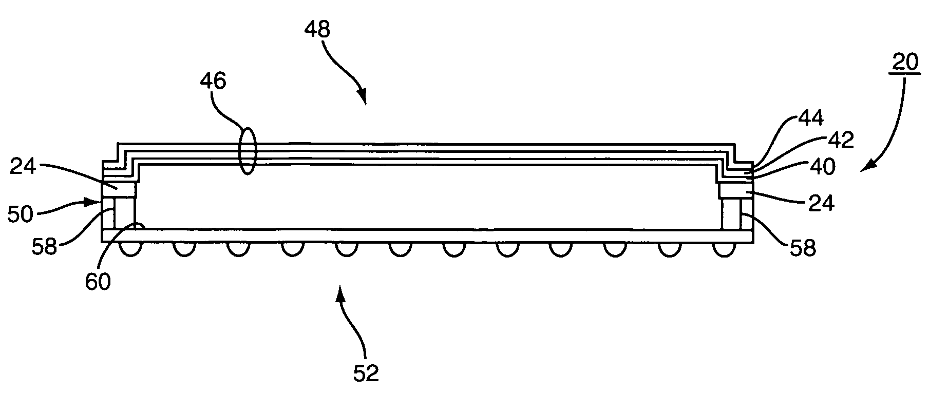
[0022] The present invention is directed to providing improved manufacturing techniques to shield an electronic module. While the present invention is particularly contemplated as being appropriate for a transceiver module, the present invention could be used with any number of different electronic modules. The manufacturing techniques of the present invention insert a conductive element around the periphery of the electronic mo...


PUM

PropertyMeasurementUnit
Electrical conductoraaaaaaaaaa

Abstract

An electromagnetic shield for an electronic module includes a surface finish that is applied to the surface of an electronic module so as to minimize the size of the shield. Once the shield is in place, the shield acts to address electromagnetic interference (EMI) concerns associated with the electronic module. An electronic module having a ring of conductive material embedded about its peripheral edge is formed. The electronic module is then sub-diced so as to expose the ring of conductive material. After sub-dicing, a conductive material may be applied through an electroless plating process followed by an electrolytic plating process. Alternatively, a conductive epoxy may be sprayed or painted onto the surface of the electronic module.

Description

FIELD OF THE INVENTION [0001] The present invention relates to a shield for an electronic module, wherein the shield is designed to reduce electromagnetic interference experienced by the electronic module. BACKGROUND OF THE INVENTION [0002] Electronic components have become ubiquitous in modern society. The electronics industry proudly, but routinely, announces accelerated clocking speeds and smaller integrated circuit modules. While the benefits of these devices are myriad, smaller and faster electronic devices create problems. In particular, high clock speeds inherently require fast transitions between signal levels. Fast transitions between signal levels create electromagnetic emissions throughout the electromagnetic spectrum. Such emissions are regulated by the Federal Communications Commission (FCC) and other regulatory agencies. Furthermore, fast speed inherently means higher frequencies. Higher frequencies mean shorter wavelengths. Shorter wavelengths mean shorter conductive ...

Claims


Application Information

Patent Timeline
IPC IPC(8): H05K9/00H01L23/552
CPCC23C30/00Y10T29/49117C25D7/00H01L23/3135H01L23/544H01L23/552H01L24/97H01L2223/54473H01L2924/01013H01L2924/01029H01L2924/0103H01L2924/01046H01L2924/01047H01L2924/01078H01L2924/01079H01L2924/14H01L2924/3025H01L2924/01006H01L2924/01033C23C28/023Y10T29/49144Y10T29/4913C25D5/12
Inventor MORRIS, THOMAS SCOTTSHAH, MILINDLEAHY, DONALD JOSEPHLAW, LEWIS KERMIT II
Owner QORVO US INC
Why Eureka
Try Eureka