

System and method of fabricating micro cavities
a technology of micro-cavities and manufacturing methods, applied in the direction of fluid pressure measurement, fluid pressure measurement by electric/magnetic elements, instruments, etc., can solve the problems of vacuum or hermetic packaging taking more than 50% of the total cost of a mems device, significant deterrent to military and commercial application of many of these devices, and deformation after deformation, etc., to achieve high density
- Summary
- Abstract
- Description
- Claims
- Application Information
AI Technical Summary
Problems solved by technology
Method used
Image

Examples
Embodiment Construction
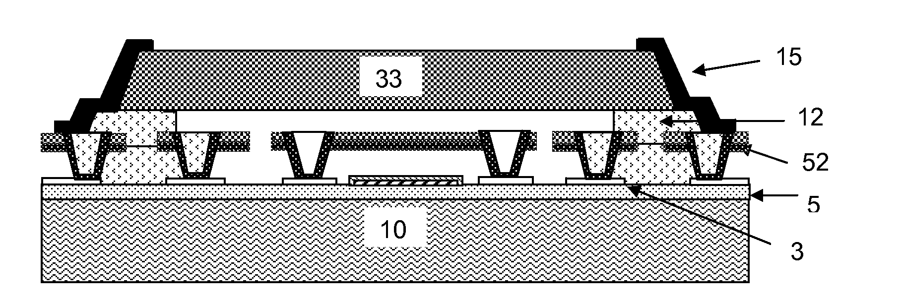
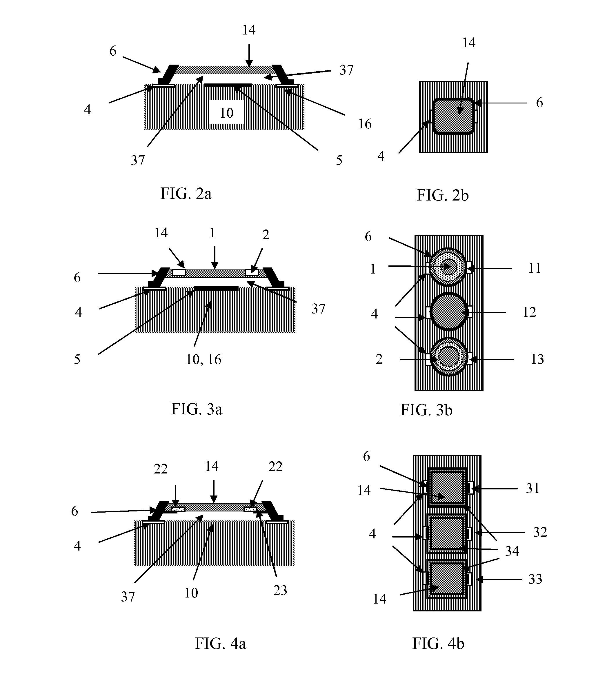
[0060]Referring to the drawings, reference is made to FIG. 2a and FIG. 2b, wherein the micro cavity embodiment that the present invention of fabrication process is capable of making is depicted in top view (FIG. 2a) and cross section view (FIG. 2b). The micro vacuum cavity 37 is formed with silicon membrane 14 as cap, metal 6 as sidewall and integrated circuits 16 as substrate 10. Contact 4 on integrated circuits 16 makes electrical contact to metal 6, which in turn makes electrical contact to silicon membrane 14. Electrode 5 on integrated circuits 16 and silicon membrane 14 form a sense capacitor.
[0061]Referring now to FIG. 5a to FIG. 5h, there is depicted cross sectional views showing a particular portion of a microstructure during specific phases of the fabrication process for the vacuum cavity 3 in FIG. 2. The thickness and gaps are not shown to scale.
[0062]FIG. 5a is cross sectional view of substrate wafer 10 comprising electrical components such as readout IC 16 and metal cont...
PUM
| Property | Measurement | Unit |
|---|---|---|
| sensitivity | aaaaa | aaaaa |
| coverage | aaaaa | aaaaa |
| stiffness | aaaaa | aaaaa |
Abstract
Description
Claims
Application Information