Layout of semiconductor device

a semiconductor device and chip technology, applied in the direction of semiconductor devices, electrical appliances, transistors, etc., can solve problems such as seriousness, and achieve the effect of shortening the channel length of the semiconductor devi

Active Publication Date: 2012-12-25
SK HYNIX INC
View PDF69 Cites 8 Cited by
  • Summary
  • Abstract
  • Description
  • Claims
  • Application Information

AI Technical Summary

Benefits of technology

[0011]Various embodiments of the present invention are directed to provide a semiconductor device layout that substantially obviates limitations and disadvantages of the related art. According to the related art in which two transistors are formed in one active region, electrical connection between a word line and a landing plug may easily occur and this problem becomes more serious as a channel length of a semiconductor device becomes shorter.
[0014]an isolation region separating the first active region and the second active region. The active region having the above-mentioned shapes increases a margin, resulting in the prevention of a bridge encountered between neighboring landing plugs.

Problems solved by technology

According to the related art in which two transistors are formed in one active region, electrical connection between a word line and a landing plug may easily occur and this problem becomes more serious as a channel length of a semiconductor device becomes shorter.

Method used


Image

  • Layout of semiconductor device
  • Layout of semiconductor device
  • Layout of semiconductor device

Examples


Embodiment Construction

[0049]Reference will now be made in detail to the embodiments of the present invention, examples of which are illustrated in the accompanying drawings. Wherever possible, the same reference numbers will be used throughout the drawings to refer to the same or like element.

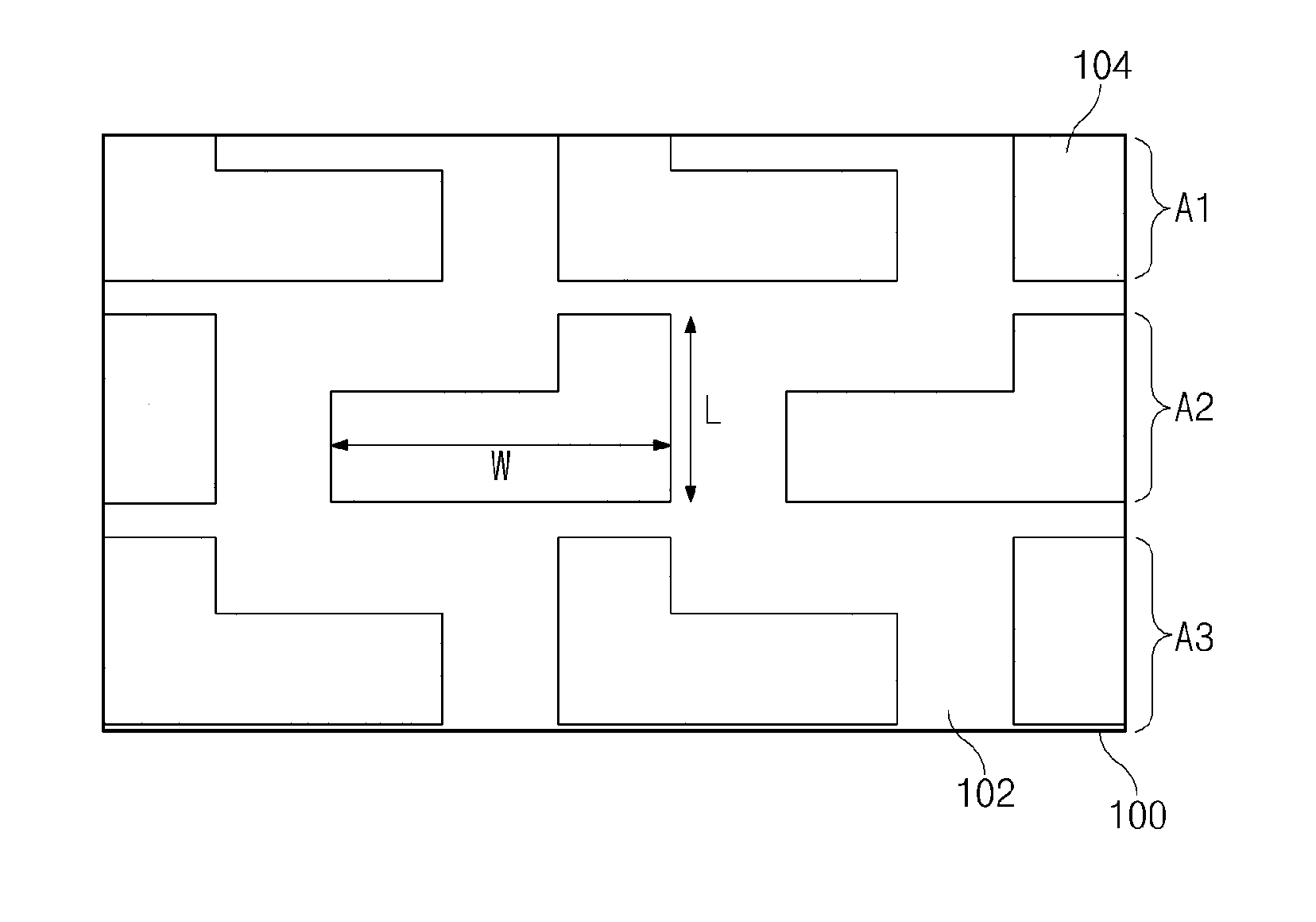
[0050]FIGS. 3A to 3G illustrate the layouts of a semiconductor device according to embodiments of the present invention.

[0051]Referring to FIG. 3a, an active regions 104 defined by a device isolation layer 102 is formed on a semiconductor substrate 100. In this case, the active region 104 is formed to have an “L”-shaped structure in which a vertical axis (L) is short and a horizontal axis (W) is relatively long. In another embodiment, the vertical axis may be long and the horizontal axis is short. In yet another embodiment, the vertical axis and the horizontal axis is substantially the same.

[0052]In the present embodiment, neighboring rows in a vertical direction are symmetrical to each other with respect to the ver...


PUM


Abstract

A layout of a semiconductor device is disclosed, which forms one transistor in one active region to reduce the number of occurrences of a bridge encountered between neighboring layers, thereby improving characteristics of the semiconductor device. Specifically, the landing plug connected to the bit line contact is reduced in size, so that a process margin of word lines is increased to increase a channel length, thereby reducing the number of occurrences of a bridge encountered between the landing plug and the word line.

Description

CROSS-REFERENCE TO RELATED APPLICATION[0001]The priority of Korean patent application No. 10-2009-0000423 filed Jan. 5, 2009, the disclosure of which is hereby incorporated in its entirety by reference, is claimed.BACKGROUND OF THE INVENTION[0002]The present invention relates to a layout of a semiconductor device.[0003]Generally, a semiconductor device forms two transistors in one active region using an active region of I-type or G-type, so that it results in a “one active region and two capacitors therein” structure. However, the “one active region and two capacitors therein” structure encounters a bridge problem between neighboring patterns so that it unavoidably deteriorates characteristics of a semiconductor device. In more detail, with the increasing degree of integration of a semiconductor device, higher-aspect-ratio patterns are laminated in the semiconductor device. In this case, some patterns fall down so that they bridge neighboring patterns, resulting in a deterioration o...

Claims


Application Information

Patent Timeline
Patent Type & Authority Patents(United States)
IPC IPC(8): H01L27/108
CPCH01L27/0207H10B12/0335H10B12/05H10B12/488H10B12/485H01L21/18
Inventor KIM, SANG HEON
Owner SK HYNIX INC
Why Eureka
Try Eureka