Semiconductor device and method for fabricating the same

a technology of metal insulation and semiconductors, applied in the direction of semiconductor devices, basic electric elements, electrical equipment, etc., can solve the problem of disadvantageous difficulty in achieving the desired threshold voltage vt, and achieve the effect of reducing the curren

Inactive Publication Date: 2006-07-20
PANASONIC CORP
View PDF4 Cites 4 Cited by
  • Summary
  • Abstract
  • Description
  • Claims
  • Application Information

AI Technical Summary

Benefits of technology

[0036] Thus, the portion of the second semiconductor region working as the channel region is in contact with the fifth semiconductor region including the first conductivity type impurity in a relatively low while it is away from the fourth semiconductor region including the first conductivity type impurity in a relatively high concentration. Therefore, an on current can be reduced.

Problems solved by technology

As a result, the concentration of the impurity in the channel regions is difficult to control, and hence, it is disadvantageously difficult to attain a desired threshold voltage Vt.

Method used


Image

  • Semiconductor device and method for fabricating the same
  • Semiconductor device and method for fabricating the same
  • Semiconductor device and method for fabricating the same

Examples


embodiment 1

[0052]—Structure of Semiconductor Device—

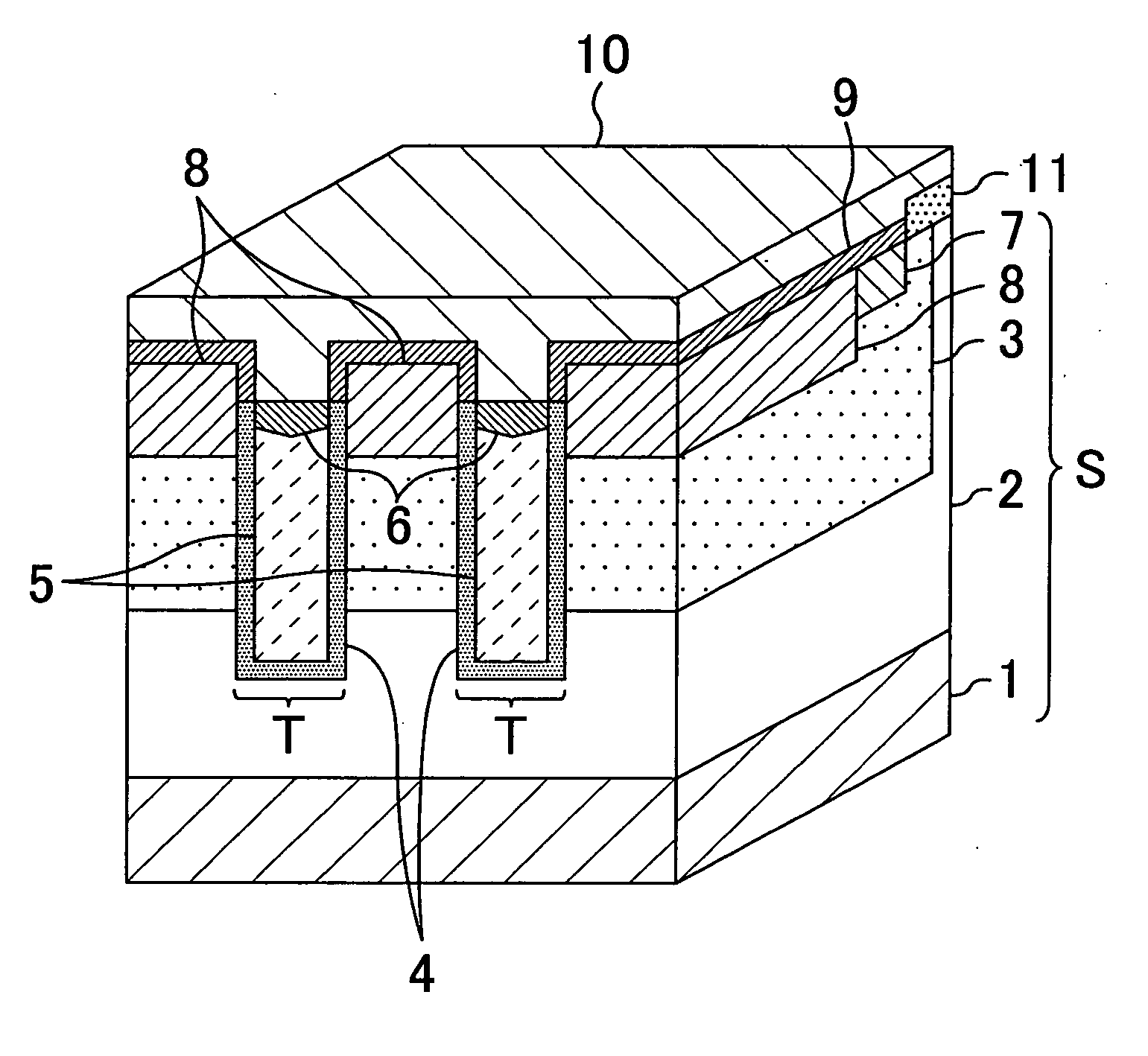
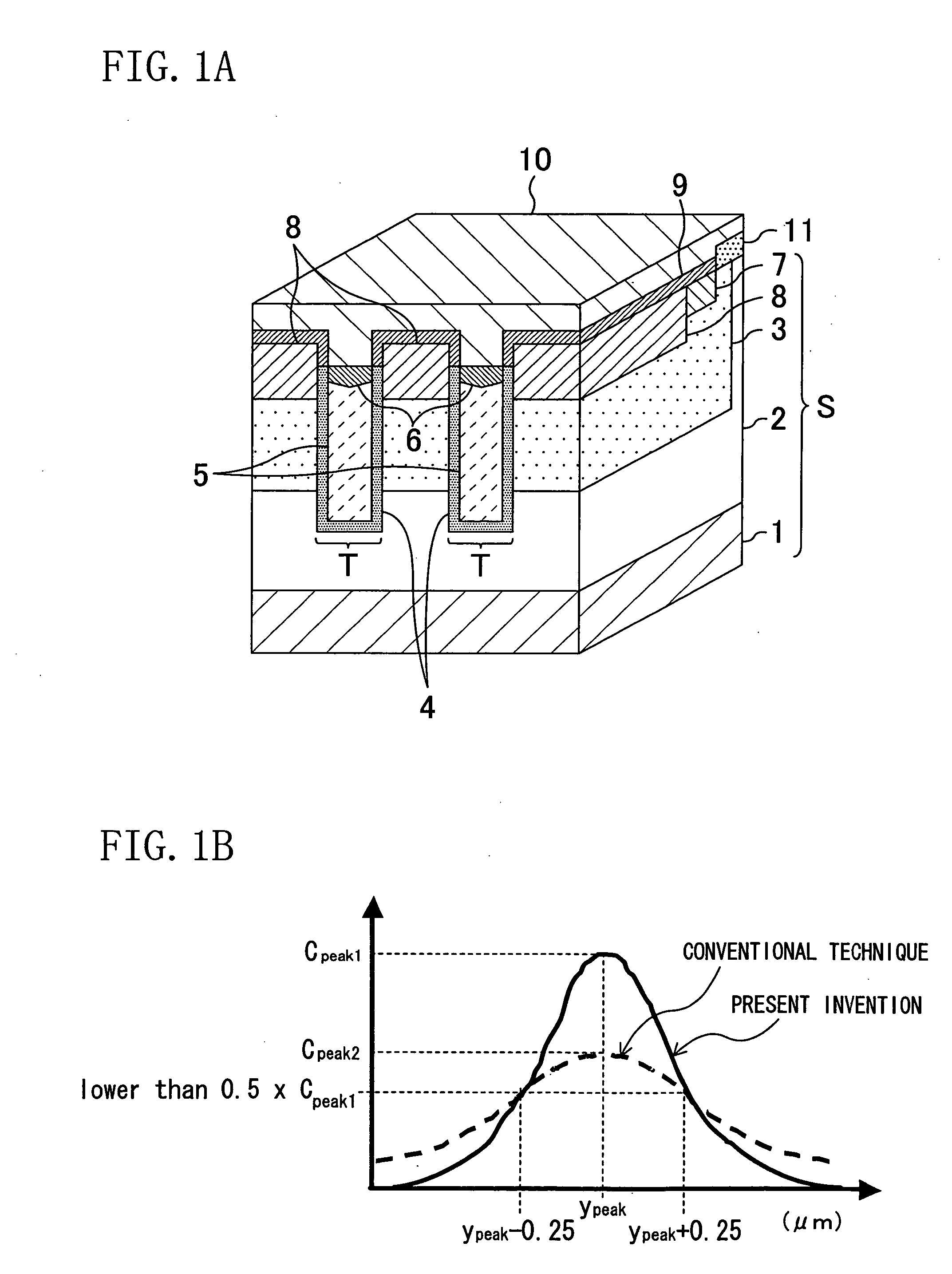
[0053]FIG. 1A is a perspective view of a semiconductor device having a trench gate structure according to Embodiment 1 of the invention, and FIG. 1B is a diagram of a concentration profile of an impurity of a second conductivity type along the vertical direction of the semiconductor device of FIG. 1A. In FIG. 1A, a barrier metal layer provided below a contact electrode 10 is omitted so that the structure can be clearly understood.

[0054] As shown in FIG. 1A, the semiconductor device of this embodiment includes a high concentration N-type drain region 1 formed at least in a region in the vicinity of the back surface of a semiconductor substrate S of silicon, a low concentration N-type drain region 2 formed on the high concentration N-type drain region 1 in the semiconductor substrate S, a P-type substrate region 3 selectively provided on the low concentration N-type drain region 2 in the semiconductor substrate S, a high concentration N-type s...

embodiment 2

[0091]—Structure of Semiconductor Device—

[0092] A semiconductor device having a trench gate structure according to Embodiment 2 of the invention has the structure shown in FIG. 1A in the same manner as in Embodiment 1.

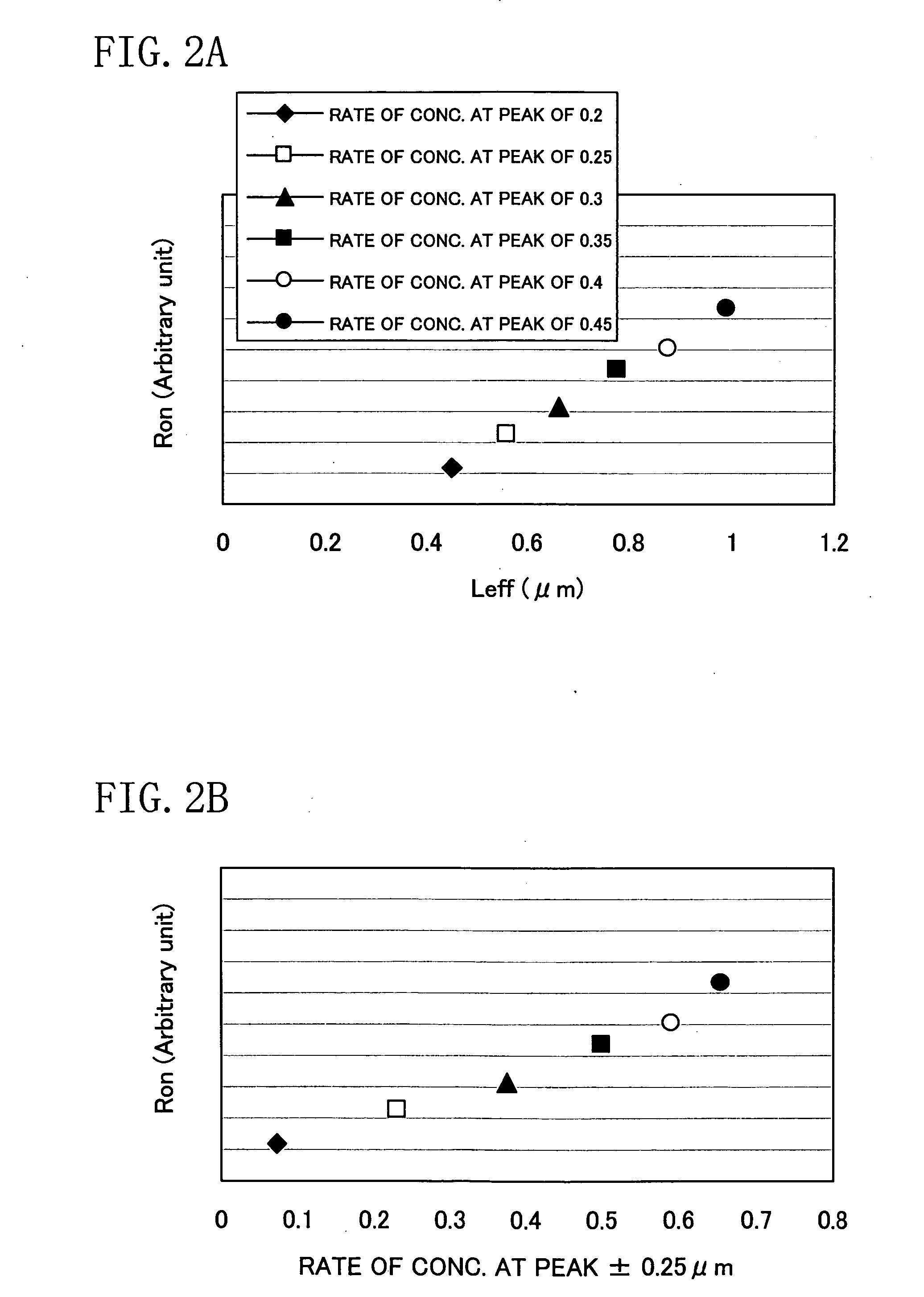
[0093] A difference of this embodiment from Embodiment 1 is a concentration profile of the second conductivity type impurity along the vertical direction of the semiconductor device of FIG. A.

[0094]FIG. 7 shows a concentration profile along the depth direction of the impurity of the second conductivity type (the P-type) determining the threshold voltage Vt in the portion of the P-type substrate region 3 sandwiched between the adjacent trenches T.

[0095] As shown in FIG. 7, a profile having two peaks are formed by introducing the second conductivity type impurity into the semiconductor substrate S through two ion implantations in this embodiment, and thus, the threshold voltage Vt is determined.

[0096] In the case where two profiles corresponding to two peaks are comp...

embodiment 3

[0107]—Structure of Semiconductor Device—

[0108] A semiconductor device having a trench gate structure according to Embodiment 3 of the invention has the structure shown in FIG. 1A in the same manner as in Embodiment 1.

[0109] A difference of this embodiment from Embodiment 1 is a concentration profile of the second conductivity type impurity along the vertical direction of the semiconductor device of FIG. 1A.

[0110]FIG. 8 shows a concentration profile along the depth direction of the impurity of the second conductivity type (the P-type) determining the threshold voltage Vt in the portion of the P-type substrate region 3 sandwiched between the adjacent trenches T.

[0111] As shown in FIG. 8, a profile having three peaks are formed by introducing the second conductivity type impurity into the semiconductor substrate S through three ion implantations in this embodiment, and thus, the threshold voltage Vt is determined.

[0112] In the case where a plurality of profiles corresponding to a ...


PUM


Abstract

After forming a first semiconductor region of a first conductivity type in a semiconductor substrate, a trench reaching a given portion of the first semiconductor region is formed in the semiconductor substrate. Then, after forming a gate insulating film on an inner wall of the trench, a second semiconductor region of a second conductivity type is formed on the first semiconductor region in the semiconductor substrate, and thereafter, a third semiconductor region of the first conductivity type is formed on the second semiconductor region in the semiconductor substrate. Also, a gate electrode of the first conductivity type is formed on the gate insulating film within the trench. The gate electrode is formed on the gate insulating film so as to extend over the second semiconductor region, a portion of the first semiconductor region disposed below the second semiconductor region and a portion of the third semiconductor region disposed on the second semiconductor region.

Description

CROSS-REFERENCE TO RELATED APPLICATIONS [0001] This application claims priority under 35 U.S.C. §119 on Patent Application No. 2005-011287 filed in Japan on Jan. 19, 2005, the entire contents of which are hereby incorporated by reference. The entire contents of Patent Application No. 2005-244253 filed in Japan on Aug. 25, 2005 are also incorporated by reference. BACKGROUND OF THE INVENTION [0002] The present invention relates to a semiconductor device having a trench MIS (Metal-Insulator-Semiconductor) gate structure and a method for fabricating the same. [0003] A trench gate structure formed by filling a gate electrode in a trench formed in a semiconductor substrate is conventionally applied to semiconductor devices such as an IGBT (Insulated Gate Bipolar Transistor) and a MISFET (Field Effect Transistor), and is advantageous for power supply and the like in particular. For example, an IGBT having a trench gate structure has both a high input impedance characteristic of a MISFET an...

Claims


Application Information

Patent Timeline
Patent Type & Authority Applications(United States)
IPC IPC(8): H01L21/336
CPCH01L29/1095H01L29/41766H01L29/4236H01L29/456H01L29/66348H01L29/66666H01L29/66727H01L29/66734H01L29/7397H01L29/7813H01L29/7827
Inventor MIYATA, SATOEMIZOKUCHI, SHUJI
Owner PANASONIC CORP
Why Eureka
Try Eureka