Manufacturing method of semiconductor device

a manufacturing method and semiconductor technology, applied in semiconductor devices, instruments, electrical devices, etc., can solve the problems of poor coverage of the semiconductor layer, the difficulty of achieving sufficient miniaturization at submicron level, and the defect generated in the manufacturing process becomes a major problem, so as to achieve the effect of short channel length of the transistor, easy realization of large size, and increased surface flatness

Inactive Publication Date: 2013-04-30
SEMICON ENERGY LAB CO LTD
View PDF137 Cites 7 Cited by
  • Summary
  • Abstract
  • Description
  • Claims
  • Application Information

AI Technical Summary

Benefits of technology

[0020]In order to make use of characteristics of an oxide semiconductor such as a light-transmitting property or an advantage that a transistor including an oxide semiconductor can easily have a large size, a glass substrate or the like is sometimes used as a substrate over which a transistor including an oxide semiconductor is formed. However, the difference in height of a surface of the glass substrate is about several tens of micrometers at a maximum, which is large as compared to the case of a silicon wafer or the like. Therefore, the accuracy of photomask projection exposure in semiconductor processing in the case of using a glass substrate is lower than that in the case of using a silicon wafer or the like, and the actual minimum feature size in the case of using a glass substrate is several micrometers at most.
[0045]In an embodiment of the invention disclosed herein, the channel length of the transistor can be sufficiently made short regardless of the kind of substrate. Therefore, it is possible to provide a semiconductor device which fully utilizes characteristics of an oxide semiconductor or an advantage attributed to the characteristics (e.g., an advantage of easily realizing large size).
[0046]In an embodiment of the invention disclosed herein, a channel formation region of a transistor is provided over a highly flat region. This makes it possible to prevent a problem such as a short channel effect even under a situation where the channel length of a transistor is short; accordingly, a transistor having favorable characteristics can be provided.
[0047]The increase in flatness of the surface over which the transistor is formed can make the thickness distribution of the oxide semiconductor film uniform; therefore, characteristics of the transistor can be improved. In addition, a decrease in coverage which may be caused by a large difference in height can be suppressed, and a break (disconnection) due to a step or a defective connection of the oxide semiconductor film can be prevented.

Problems solved by technology

In the case of using an exposure apparatus for glass substrates (also referred to as a stepper), the above-described limit of the feature size makes it difficult to achieve sufficient miniaturization at submicron level.
In the case where a transistor is miniaturized, a defect generated in the manufacturing process becomes a major problem.
For example, in a transistor where a semiconductor layer is formed over a wiring functioning as a source or drain electrode, a gate electrode or the like, the wiring has a larger thickness than the semiconductor layer, which causes poor coverage with the semiconductor layer when the thickness of the semiconductor layer is reduced along with miniaturization.
As a result, disconnection, a defective connection, or the like may occur.
Further, in the case where the channel length of a transistor is short, another problem of a short channel effect arises.
The short channel effect is likely to occur particularly in a transistor including an oxide semiconductor because the threshold voltage of such a transistor cannot be controlled by doping, unlike a transistor including silicon.

Method used


Image

  • Manufacturing method of semiconductor device
  • Manufacturing method of semiconductor device
  • Manufacturing method of semiconductor device

Examples


embodiment 1

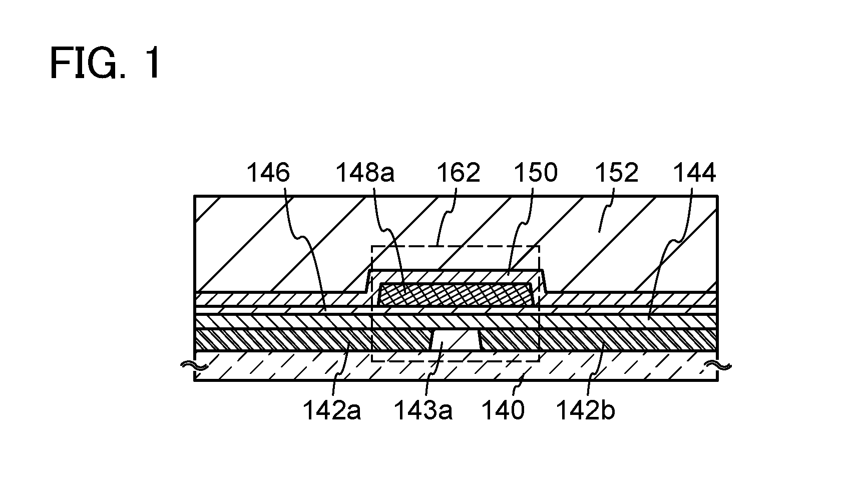
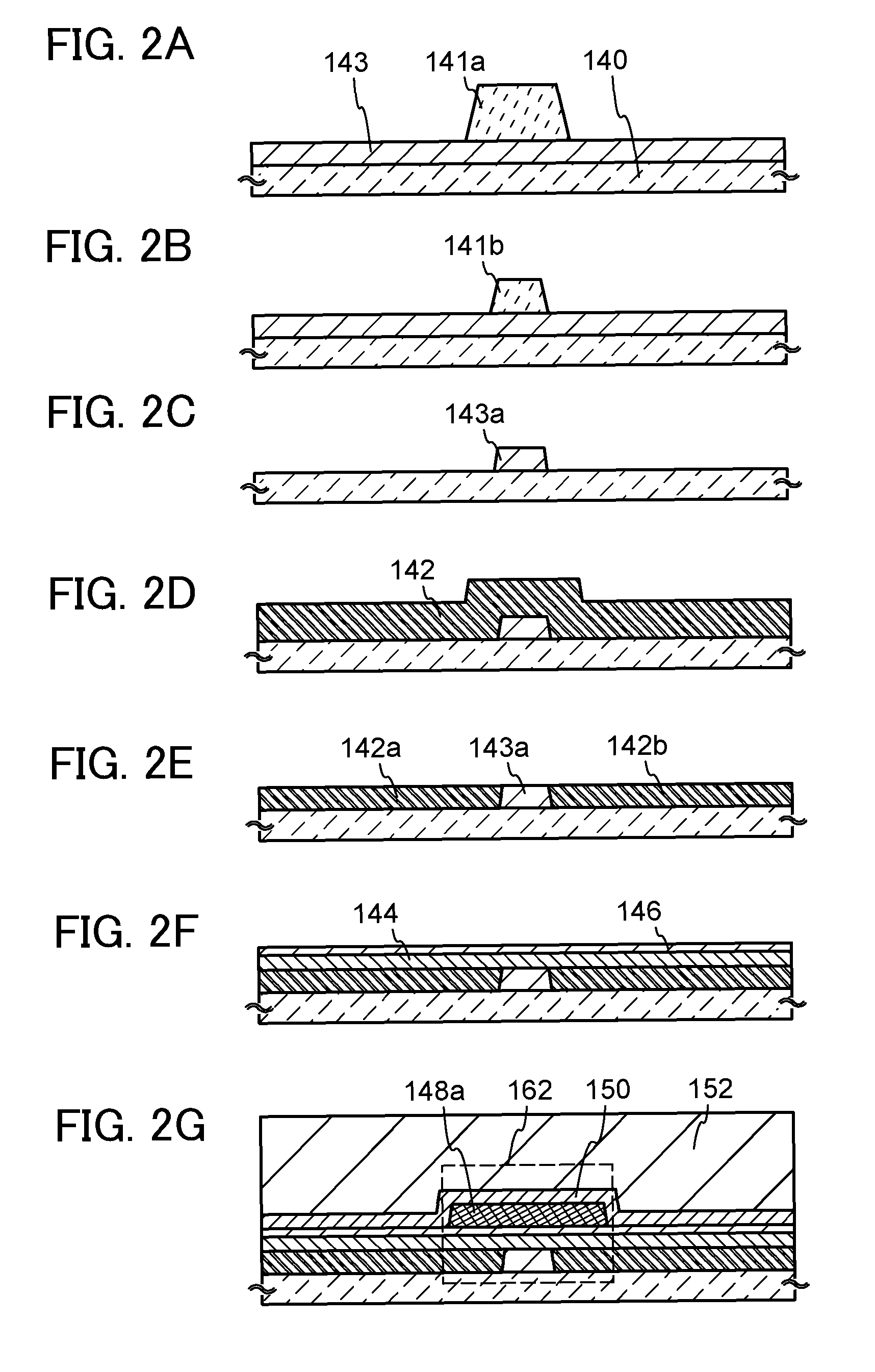
[0070]In this embodiment, a structure and a manufacturing method of a semiconductor device according to an embodiment of the invention disclosed herein will be described with reference to FIG. 1 and FIGS. 2A to 2G

[0071]FIG. 1 illustrates an example of the structure of a semiconductor device.

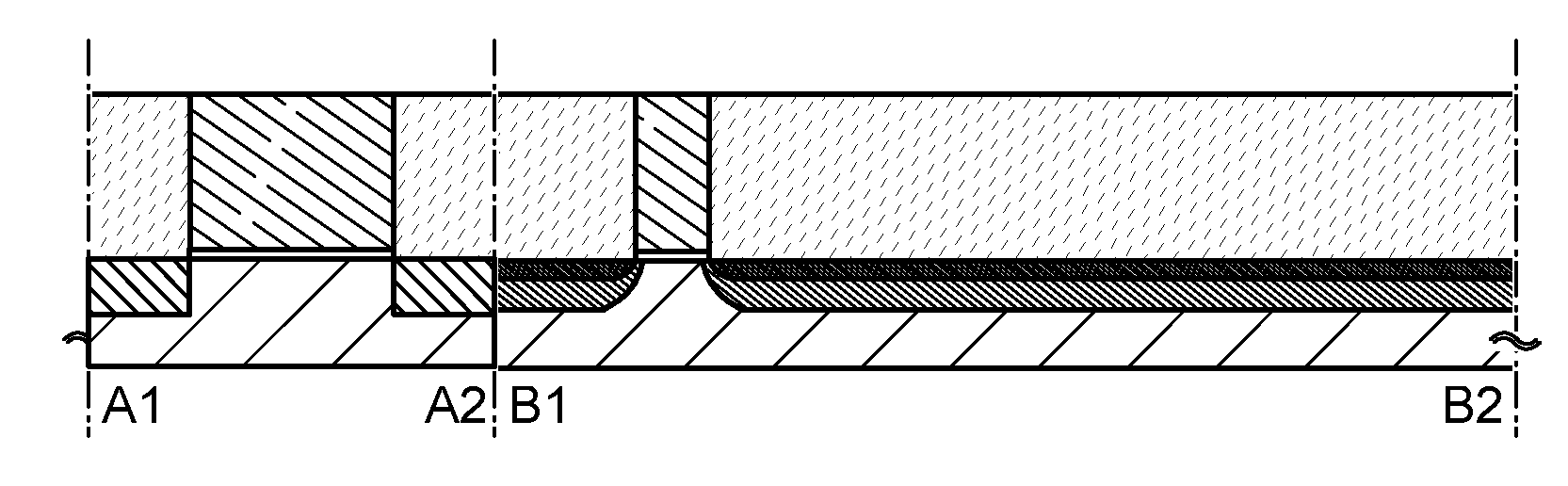
[0072]A transistor 162 in FIG. 1 includes an insulating film 143a over a substrate 140 having a surface over which components are formed, a source electrode 142a and a drain electrode 142b between which the insulating film 143a is sandwiched, an oxide semiconductor film 144 in contact with a part of an upper surface of the insulating film 143a, a part of an upper surface of the source electrode 142a, and a part of an upper surface of the drain electrode 142b, a gate insulating film 146 covering the oxide semiconductor film 144, and a gate electrode 148a over the gate insulating film 146.

[0073]The channel length of the transistor 162 is preferably less than 2 μm, further preferably greater than or...

embodiment 2

[0141]In this embodiment, a structure and a manufacturing method of a semiconductor device according to another embodiment of the invention disclosed herein will be described with reference to FIGS. 3A to 3C, FIGS. 4A to 4D, and FIGS. 5A to 5C.

[0142]FIGS. 3A to 3C illustrate an example of a structure of a semiconductor device. FIG. 3A is a cross-sectional view of the semiconductor device; FIG. 3B is a plan view of the semiconductor device; and FIG. 3C illustrates a circuit configuration of the semiconductor device. Note that a structure of the semiconductor device is mainly described in this embodiment, and operation of the semiconductor device will be described in detail in the following embodiment. Note that the semiconductor device illustrated in FIGS. 3A to 3C is just an example of a semiconductor device having a predetermined function and does not exhaustively represent the semiconductor device of the invention disclosed herein. The semiconductor device according to the inventi...

embodiment 3

[0175]In this embodiment, an example of application of a semiconductor device according to one embodiment of the invention disclosed herein will be described with reference to FIGS. 6A, 6B, and 6C. Here, an example of a memory device will be described. Note that in some circuit diagrams, “OS” is written beside a transistor in order to indicate that the transistor includes an oxide semiconductor.

[0176]In a semiconductor device which can be used as a memory device, which is illustrated in FIG. 6A, a first wiring (1st Line) is electrically connected to a source electrode (or a drain electrode) of a transistor 1000. A second wiring (2nd Line) is electrically connected to a drain electrode (or a source electrode) of the transistor 1000. A third wiring (3rd Line) is electrically connected to a source electrode (or a drain electrode) of a transistor 1010. A fourth wiring (4th Line) is electrically connected to a gate electrode of the transistor 1010. Furthermore, a gate electrode of the tr...


PUM


Abstract

An embodiment is a manufacturing method of a semiconductor device including the steps of forming a first insulating film; forming a first mask over the first insulating film; performing a slimming process on the first mask to form a second mask; performing an etching process on the first insulating film using the second mask to form a second insulating film; forming a first conductive film covering the second insulating film; performing a polishing process on the first conductive film and the second insulating film to form a third insulating film, a source electrode, and a drain electrode having equal thicknesses; forming an oxide semiconductor film over the third insulating film, the source electrode, and the drain electrode; forming a gate insulating film over the oxide semiconductor film; and forming a gate electrode in a region which is over the gate insulating film and overlaps with the third insulating film.

Description

TECHNICAL FIELD[0001]The technical field of the present invention relates to a semiconductor device and a manufacturing method of the semiconductor device. Here, semiconductor devices refer to general elements and devices which function utilizing semiconductor characteristics.BACKGROUND ART[0002]There are a wide variety of metal oxides and such metal oxides are used for various applications. Indium oxide is a well-known material and has been used for transparent electrodes required in liquid crystal display devices or the like.[0003]Some metal oxides have semiconductor characteristics. Examples of such metal oxides having semiconductor characteristics are tungsten oxide, tin oxide, indium oxide, zinc oxide, and the like. Thin film transistors in which a channel formation region is formed using such metal oxides are already known (e.g., see Patent Documents 1 to 4, Non-Patent Document 1, and the like).[0004]As metal oxides, not only single-component oxides but also multi-component ox...

Claims


Application Information

Patent Timeline
Patent Type & Authority Patents(United States)
IPC IPC(8): H01L21/336
CPCG11C16/0433H01L27/0688H01L27/11521H01L27/11551H01L27/1156H01L27/1288H01L27/1225H01L29/78636H01L29/7869H01L29/66969H01L27/1214H10B41/70H10B41/20H10B41/30
Inventor SUZAWA, HIDEOMISASAGAWA, SHINYA
Owner SEMICON ENERGY LAB CO LTD
Why Eureka
Try Eureka