High current density power field effect transistor

a high current density, transistor technology, applied in the direction of semiconductor devices, basic electric elements, electrical appliances, etc., can solve the problems of less total switching efficiency improvement, negative total switching efficiency in dc-dc conversion, and all solutions have their own drawbacks, so as to achieve lower forward voltage (vf), high density power field, and short channel length

Active Publication Date: 2012-09-18
VISHAY SILICONIX LLC
View PDF14 Cites 6 Cited by
  • Summary
  • Abstract
  • Description
  • Claims
  • Application Information

AI Technical Summary

Benefits of technology

[0009]Embodiments of the present invention implement high density power field effect transistor that avoids the channel mobility problems caused by gate oxide scattering, that exhibits lower forward voltage (Vf) rated at high current; and that shows shorter channel length for faster switching. This invention can apply to DC-DC conversion as a synchronized rectifier transistor.
[0010]In one embodiment, the present invention is implemented as a power field effect transistor device. The device includes a Schottky diode formed in a vertical trench contact, a junction FET (JFET) component, a first accumulation MOSFET disposed adjacent to the JFET component, and a second accumulation MOSFET disposed adjacent to the JFET component on the side opposite the first accumulation MOSFET. The JFET component, the vertical Schottky and the first accumulation MOSFET are configured to provide both current path in “on” mode and voltage blocking in “off” mode. The induced current flow through bulk silicon regions of the device is configured to reduce gate oxide scattering. The second accumulation MOSFET, formed near the bottom of trench structure can also provide accumulated electrons in the current path when gate electrode is under positive bias for n-channel device, which can help to reduce on-resistance of this device.

Problems solved by technology

However, the reverse recovery from the p-n body diode in the free wheeling mode contributes adversely to the total switching efficiency in DC-DC conversion.
However, all these solutions have their own drawbacks.
For instance, the external Schottky approach can lead to high inductance, thus leading to less total switching efficiency improvement.
On the other hand, a monolithically integrated Schottky approach compromises silicon real estate usage for on-resistance reduction because of certain percentage of silicon area has to be allocated to Schottky integration, and the small area of the integrated Schottky also limits current capability and the forward voltage lowing advantage.
The irradiation approach can lead to significant changes in threshold voltage, leakage current and breakdown voltage due to the damage induced by irradiations.
From process and product complexity point of view, all these solutions are not economically sound because extra process steps need to be added, such as adding more mask layers in fabricating the devices.
Due to the process control concern, adding Schottky diode in every active cell limits the possibility for further pitch shrink opportunity, which is the critical direction for reducing on-resistance for power device in low voltage application.
The challenge is how to integrate a Schottky diode in a power device without impacting on-resistance for low voltage device applications.
However, high reverse leakage current is the most problematic drawback.
It is very hard to achieve “normally-off” characteristics when the gate is grounded.
However, one major device characteristic different from conventional power MOSFET should not be ignored when ACCUFET is used as power switching device: its bi-directional switching nature shows that the reverse and forward blocking are only kept in a finite duration because of the accumulation of minority carriers, which make the depletion width narrower.
This effect limits the effectiveness of blocking capability.
The direct connection between this p type to N+ source can help to reduce reverse leakage, however, the low on-resistance and low forward voltage advantages were not achieved.

Method used


Image

  • High current density power field effect transistor
  • High current density power field effect transistor
  • High current density power field effect transistor

Examples


Embodiment Construction

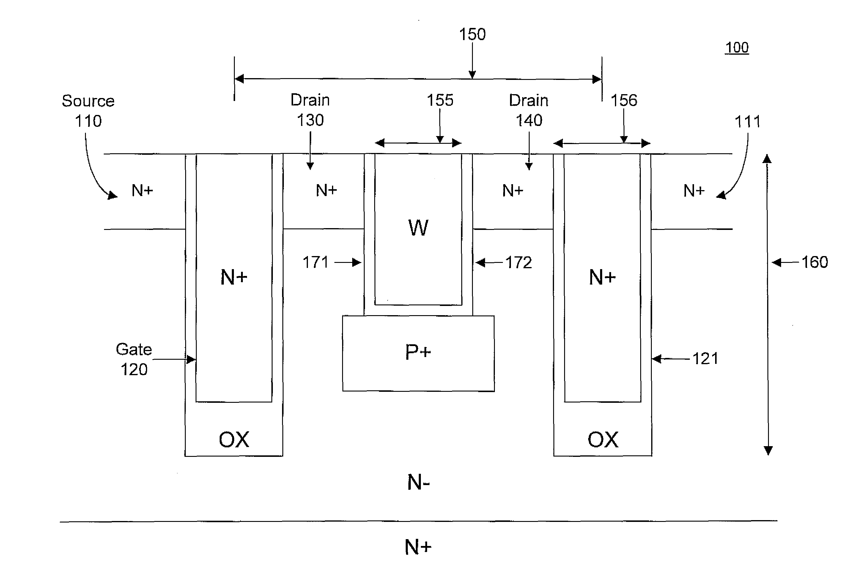
[0018]Reference will now be made in detail to the preferred embodiments of the present invention, examples of which are illustrated in the accompanying drawings. While the invention will be described in conjunction with the preferred embodiments, it will be understood that they are not intended to limit the invention to these embodiments. On the contrary, the invention is intended to cover alternatives, modifications and equivalents, which may be included within the spirit and scope of the invention as defined by the appended claims. Furthermore, in the following detailed description of embodiments of the present invention, numerous specific details are set forth in order to provide a thorough understanding of the present invention. However, it will be recognized by one of ordinary skill in the art that the present invention may be practiced without these specific details. In other instances, well-known methods, procedures, components, and circuits have not been described in detail ...


PUM


Abstract

An ultra-short channel hybrid power field effect transistor (FET) device lets current flow from bulk silicon without npn parasitic. This device does not have body but still have body diode with low forward voltage at high current rating. The device includes a JFET component, a first accumulation MOSFET disposed adjacent to the JFET component, and a second accumulation MOSFET disposed adjacent to the JFET component at the bottom of the trench end, or a MOSFET with an isolated gate connecting the source.

Description

TECHNICAL FIELD[0001]The present invention relates to trench based high current density power semiconductor structures made by vertical integration of different kinds of semiconductor devices. Its low forward voltage and on-resistance characteristics at high current allow this normally-off device used as a synchronized rectifier transistor in DC-DC conversion applicationBACKGROUND ART[0002]Power MOSFETs (metal-oxide-semiconductor field-effect transistors) comprise one of the most useful field effect transistors implemented in both analog and digital circuit applications as energy saving switches.[0003]In general, a trench-based power MOSFET is built using a vertical structure as opposed to a planar structure. The vertical structure enables the transistor to sustain both high blocking voltage and high current. Similarly, with a vertical structure, the component area and active device density are roughly proportional to the current it can sustain as a device “on” characteristics, and ...

Claims


Application Information

Patent Timeline
Patent Type & Authority Patents(United States)
IPC IPC(8): H01L27/105
CPCH01L27/085H01L29/7828H01L29/0623H01L29/407H01L29/8083H01L29/42368H01L29/47H01L29/41766
Inventor LI, JIANOWYANG, KING
Owner VISHAY SILICONIX LLC
Why Eureka
Try Eureka