Probe for testing semiconductor devices

a technology for semiconductor devices and contactors, applied in the direction of electrical testing, measurement devices, instruments, etc., can solve the problems of increasing the cost of probe cards, requiring a larger probe force, and a large tip contact area, so as to achieve the effect of increasing the packing density

Active Publication Date: 2013-01-01
FORMFACTOR INC
View PDF5 Cites 4 Cited by
  • Summary
  • Abstract
  • Description
  • Claims
  • Application Information

AI Technical Summary

Benefits of technology

[0014]The moment of inertia for the torsion and / or bending elements can be lowered, thus altering the energy absorption or distribution characteristics by making the element longer and / or narrower / thinner and also by manipulating the material used (i.e., a material with a lower Young's Modulus). Conversely, the moment of inertia can be increased by using a material that is less pliable (higher Young's Modulus) and by making the element shorter and / or wider / thicker. Also, a split bar or double-layer structure design can be used to achieve a higher moment of inertia. In yet another embodiment, the hybrid probe may use multiple materials such as one for the bending element and another for the torsion element. Fine tuning the hybrid probe through pivot placement, additional angular elements, and modifications to moments of inertia allows a probe card manufacturer to optimize a probe card for a particular application, further increasing the probe card efficiency and cost effectiveness.

Problems solved by technology

This results in a larger tip contact area and a larger probe force is thus needed to pierce the aluminum oxide layer.
When you multiply this force by the hundreds or thousands of probes on a probe card, the probe card must be engineered to accommodate significant forces, which usually means reinforcing the probe card components, which in turn increases probe card costs.
It is clear from FIGS. 8A and 8B that the stress distribution is inefficient because only small portions of the bending element absorb the stress.
And it is in these small portions where the probe is more likely to fail forcing manufacturers to widen the bending element at the probe foot to reduce stress and prevent failures.
A wider bending element near the probe base, however, adversely affects the packing density of the probe card.
This results in a smaller tip contact area and a smaller probe force is thus needed to pierce the aluminum oxide layer, which in turn, reduces the overall force exerted by the probe card.
Unfortunately though, the torsional probe too has drawbacks.
First, for a typical torsional design with a shorter geometry of the arm, the scrub length is generally longer which can limit the size of contact pads for the DUTs.
This z-deformation may be caused by material fatigue.
Third, at the union angle (where the torsional member meets a second element of the probe) there can be significant stress which can cause fractures, and thus, render the probe inoperable.
And finally a conventional torsional design has a very large footprint, meaning that the probes cannot be packed onto the substrate in high densities.
Thus there are some DUTs for which a conventional torsional design cannot be used because the DUT has contacts whose packing density is too tight.

Method used


Image

  • Probe for testing semiconductor devices
  • Probe for testing semiconductor devices
  • Probe for testing semiconductor devices

Examples


Embodiment Construction

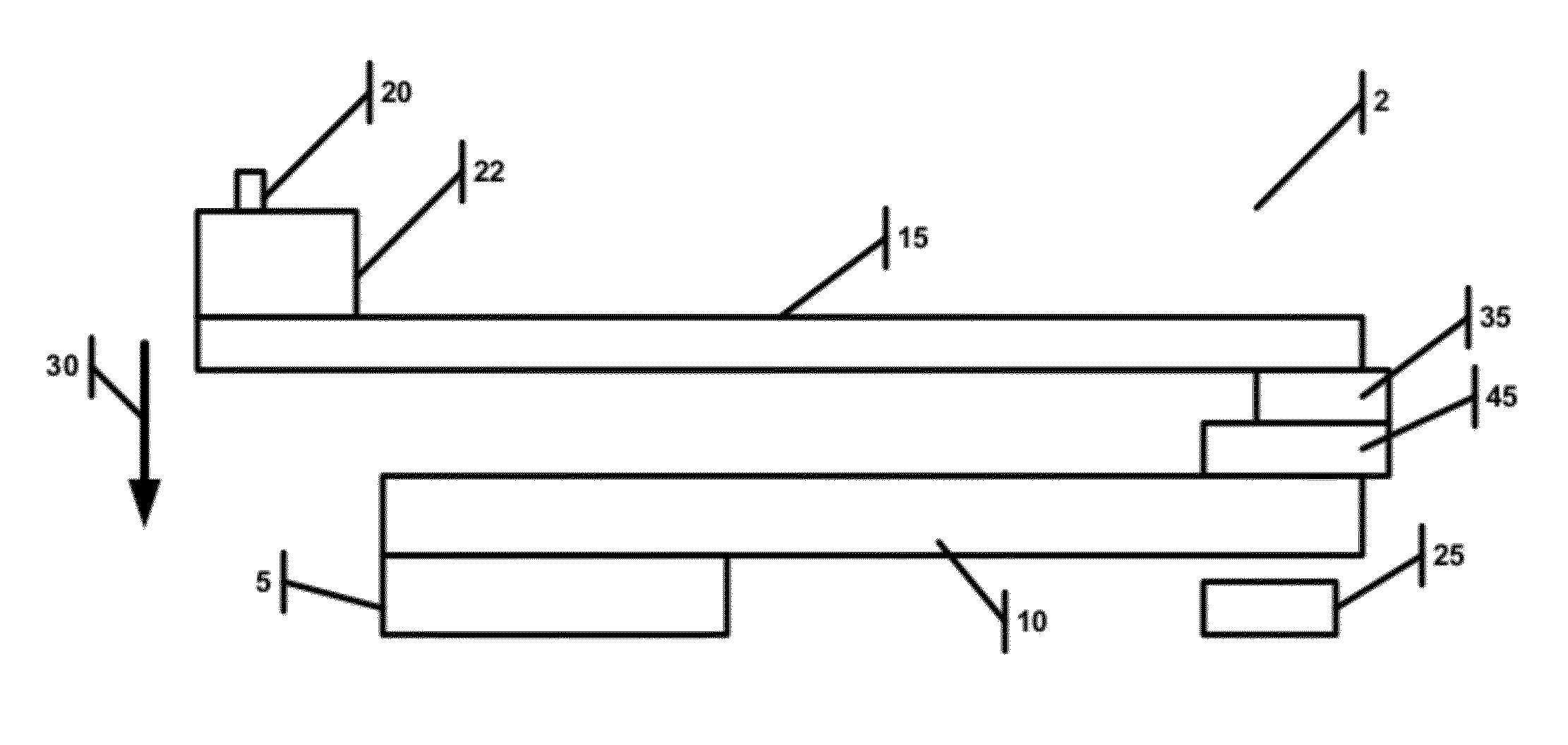
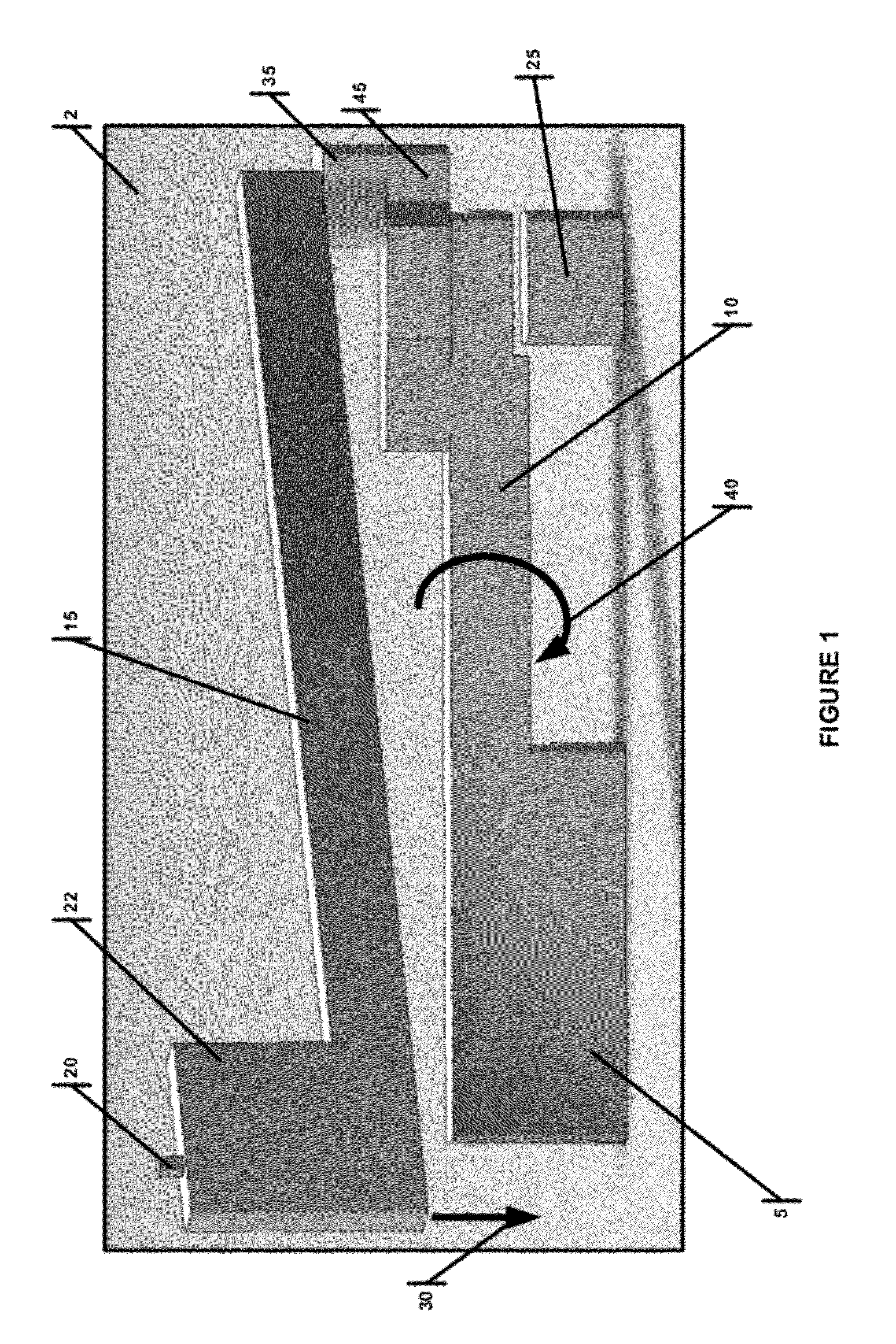
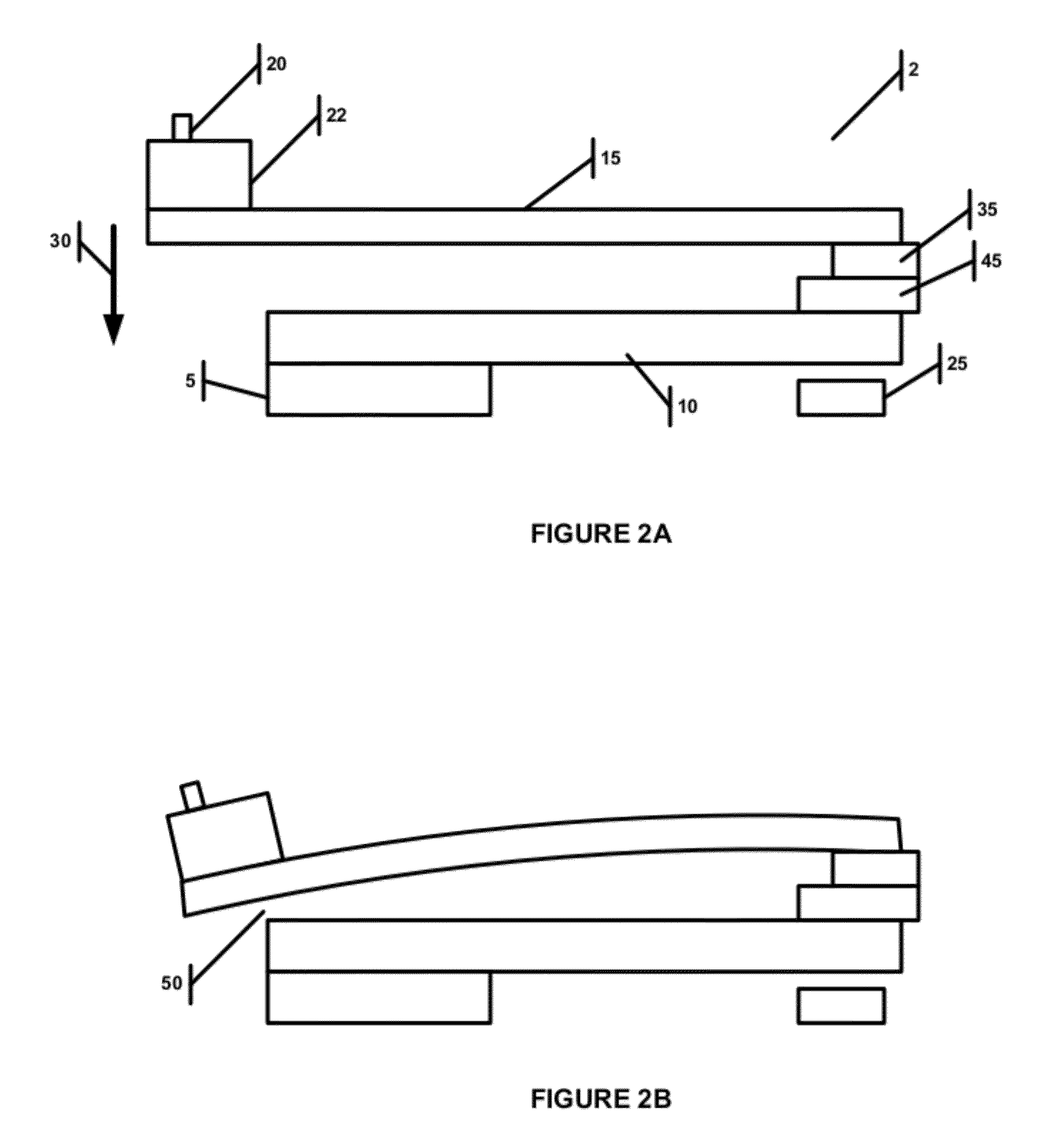
[0034]What is described below is a novel hybrid torsional probe design that has a high packing density. The design comprises a torsion element and a bending element, such that it comprises a hybrid design. Also described below are novel probe designs that incorporate various union angle interface edge shapes, pivot cutouts and buffer layers to prevent failure from stress fractures. As described in U.S. Pat. No. 7,589,542 and U.S. patent Ser. No. 12 / 042,295, of which the present application is a continuation-in-part, a hybrid torsional design is described. The following disclosure details further improvements to the previously disclosed probe designs.

[0035]Now turning to the novel torsional probe, both the torsion and bending elements allow the hybrid probe to store the displacement energy through torsion and bending. The hybrid design exploits the advantages of both the torsional and cantilever probe designs (i.e., greater packing density, less probe failure from material fatigue, l...


PUM


Abstract

A novel hybrid probe design is presented that comprises a torsion element and a bending element. These elements allow the probe to store the displacement energy as torsion or as bending. The novel hybrid probe comprises a probe base, a torsion element, a bending element, and a probe tip. The probe elastically deforms to absorb the displacement energy as the probe tip contacts the DUT contact pad. The bending element absorbs some of the displacement energy through bending. Because the torsion element and the bending element join at an angle between −90 degrees and 90 degrees, a portion of the displacement energy is transferred to the torsion element causing it to twist (torque). The torsion element can also bend to accommodate the storage of energy through torsion and bending. Also, adjusting the position of a pivot can be manipulated to alter the energy absorption characteristics of the probe. One or more additional angular elements may be added to change the energy absorption characteristics of the probe. And, the moment of inertia for the torsion and / or bending elements can by manipulated to achieve the desired probe characteristics. Other features include a various union angle interface edge shapes, pivot cutouts and buffers.

Description

1. FIELD OF THE INVENTION[0001]The present invention relates to devices for testing semiconductor devices and more particularly to the design of probe contactors for such testing.2. BACKGROUND OF THE INVENTION[0002]Integrated circuits are made in a bulk parallel process by patterning and processing semiconductor wafers. Each wafer contains many identical copies of the same integrated circuit referred to as a “die.” It may be preferable to test the semiconductor wafers before the die is cut into individual integrated circuits and packaged for sale. If defects are detected the defective die can be culled before wasting resources packaging a defective part. The individual die can also be tested after they have been cut into individual integrated circuits and packaged.[0003]To test a wafer or an individual die—commonly called the device under test or DUT—a probe card is commonly used which comes into contact with the surface of the DUT. The probe card generally contains three unique cha...

Claims


Application Information

Patent Timeline
Patent Type & Authority Patents(United States)
IPC IPC(8): G01R31/00
CPCG01R1/06727G01R1/06733
Inventor KHOO, MELVINHU, TINGLOSEY, MATTHEW
Owner FORMFACTOR INC
Why Eureka
Try Eureka