Method for manufacturing flexible display substrate and flexible display device

a technology of flexible display substrate and display device, which is applied in the manufacture of cables/conductors, electrical appliances, instruments, etc., can solve the problems of contaminated display substrate, reduced life of press, and degradation of display substrate, so as to improve the reliability of display panels and facilitate separation of unit display panels from mother substrates.

Inactive Publication Date: 2013-01-08
LG DISPLAY CO LTD
View PDF9 Cites 15 Cited by
  • Summary
  • Abstract
  • Description
  • Claims
  • Application Information

AI Technical Summary

Benefits of technology

[0018]An advantage of the present invention is to improve the reliability of a display panel and easily separate a unit display panel from a mother substrate.

Problems solved by technology

However, burrs may occur at edges of the unit display panel P in the process of cutting the mother substrate 100 using a press, degrading the quality of the display substrate.
Further, when the mother substrate 100 is thick, a cutter of the press becomes extremely worn out and thus the lifetime of the press is reduced.
Furthermore, the display substrate may be contaminated by particles generated in the process of cutting the mother substrate 100 using the press.

Method used


Image

  • Method for manufacturing flexible display substrate and flexible display device
  • Method for manufacturing flexible display substrate and flexible display device
  • Method for manufacturing flexible display substrate and flexible display device

Examples


Embodiment Construction

[0045]Reference will now be made in detail to embodiments of the present disclosure, examples of which are illustrated in the accompanying drawings.

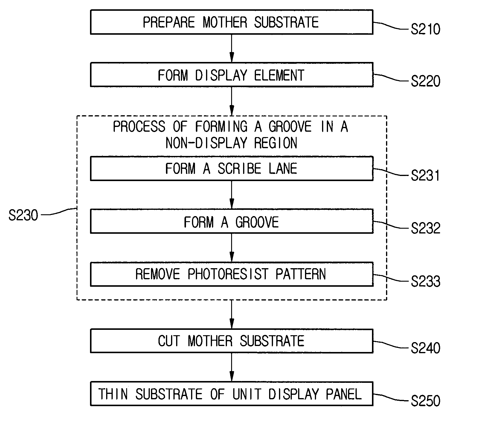
[0046]FIG. 3 is a flowchart illustrating a method for manufacturing a flexible display substrate according to an embodiment.

[0047]The method includes a process S210 of preparing a mother substrate, a process S220 of forming a display element, a process S230 of forming a groove in a non-display region, a process S240 of cutting the mother substrate, and a process S250 of thinning the substrate of a unit display panel.

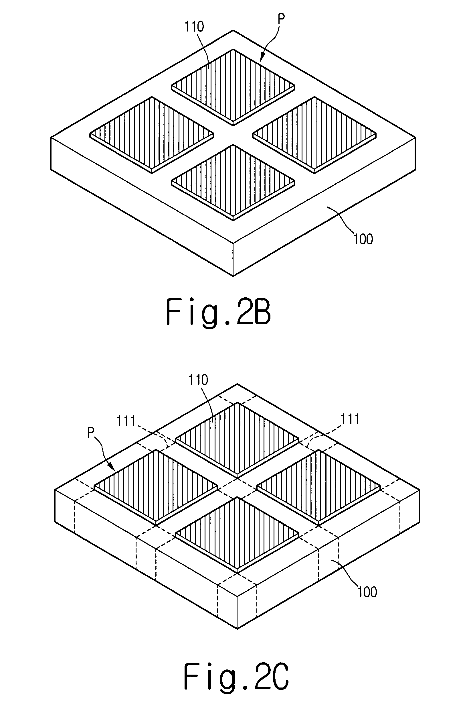
[0048]FIG. 4A is a perspective view illustrating a process of preparing a mother substrate, and FIG. 4B is a cross-sectional view illustrating the process of preparing the mother substrate illustrated in FIG. 4A.

[0049]Referring to FIGS. 3, 4A and 4B, a mother substrate 200 having a first thickness d1 is prepared (S210). The mother substrate 200 may be a metal substrate. For example, the metal substrate may be formed of stainl...


PUM

PropertyMeasurementUnit
thicknessaaaaaaaaaa
thickness d1aaaaaaaaaa
thicknessaaaaaaaaaa

Abstract

A method for manufacturing a flexible electrophoretic display device, including: providing a metal mother substrate having a first thickness, including a unit display panel region and a non-display region adjacent the unit display panel region; forming a display element in the unit display panel region; forming a groove in the non-display region of the mother substrate; cutting the mother substrate along the groove to separate the unit display panel region from the mother substrate; thinning the substrate of the separated unit display panel region; and forming an electrophoretic ink film on the unit display panel region.

Description

[0001]This application claims the benefit of Korean Patent Application No. 10-2007-0044823, filed on May 9, 2007, which is hereby incorporated by reference for all purposes as if fully set forth herein.BACKGROUND OF THE INVENTION[0002]1. Field of the Invention[0003]The present invention relates to a method for manufacturing a flexible display substrate and flexible display device.[0004]2. Discussion of the Related Art[0005]As the information society becomes more advanced, a variety of flat display devices have been developed. Examples of flat display devices include liquid crystal display (LCD) devices, plasma display panel (PDP) devices, electro-luminescent display devices (ELD), and vacuum fluorescent display devices (VFD).[0006]The recent trend is that flat panel display devices are applied to portable products, e.g., electronic sheets, arm bands, wallets, notebook computers, etc. To this end, development of flexible display devices is in progress.[0007]Display devices mounted on...

Claims


Application Information

Patent Timeline
Patent Type & Authority Patents(United States)
IPC IPC(8): H01B13/00B44C1/22G02F1/167G02F1/16755
CPCG02F1/133305G02F1/133351G02F1/167G02F1/16755G02F1/13
Inventor PAEK, SEUNG HANLEE, KYOUNG MOOKKIM, SUNG HWANKIM, SU HO
Owner LG DISPLAY CO LTD
Why Eureka
Try Eureka